Highly efficient hybrid tandem white organic light-emitting diodes with two different color-emitting units
Xiao Li
1,#
,
Taiju Tsuboi
2,3,#,*

,
Lian Duan
1,4,*
*Correspondence to:
Taiju Tsuboi, Department of Polymer Science and Engineering, Zhejiang University, Hangzhou 310027, Zhejiang, China; Faculty of Engineering, Kyoto Sangyo University, Kamigamo, Kyoto 603-8555, Japan.
E-mail: tsuboi@cc.kyoto-su.ac.jp
Lian Duan, Key Laboratory of Organic Optoelectronics and Molecular Engineering of Ministry of Education, Department of Chemistry, Laboratory of Flexible Electronics Technology, Tsinghua University, Beijing 100084, China. E-mail: duanl@mail.tsinghua.edu.cn
Lian Duan, Key Laboratory of Organic Optoelectronics and Molecular Engineering of Ministry of Education, Department of Chemistry, Laboratory of Flexible Electronics Technology, Tsinghua University, Beijing 100084, China. E-mail: duanl@mail.tsinghua.edu.cn
Smart Mater Devices. 2025;1:36716. 10.70401/smd.2025.0003
Received: July 01, 2024Accepted: September 21, 2024Published: January 13, 2025
This article belongs to the Special lssue Towards High-Performance and Long-Lifetime OLEDs
Abstract
White-color organic light-emitting diodes (WOLEDs) have aroused wide interests for future lighting because of low energy consumption in principle, while still suffer from the degradation by Joule heating and polaron-induced quenching under high luminance caused by high current in practical. To obtain high current efficiency, which means high luminance at low current density, tandem WOLEDs with multiple electroluminescence (EL) units connected in series with charge generation layers (CGLs) have been developed. Here we report the improved hybrid tandem WOLED with two EL units, EL1 and EL2, where EL1 and EL2 generate fluorescent blue and phosphorescent yellow emissions from a metal-free material BCzVBi and a Ir-complex (fbi)2Ir(acac), respectively, with CGL composed of a HATCN/NPB bilayer. The white-light emitting device shows the maximum current efficiency and power efficiency of 60.2 cd/A and 29.6 lm/W, respectively, without out-coupling structure. A low driving voltage of 6.5 V at 1,000 cd/m2 is realized, which is an important value because such a luminance is required for actually employed lighting device. The blue emission appears from 5.4 V, and the light color changes from yellowish to bluish white during 5.4 V to 13.4 V, which could be explained by the energy level structures of the device and proved by the J-V characteristics. Additionally, this tandem WOLED also shows photovoltaic effect. This work provides a design of room light source whose color temperature could be tuned through applied voltage when needed, and a display system for low-current operated amorphous Si-TFT due to its high current efficiency.
Keywords
Hybrid tandem white OLED, low driving voltage, high efficiency, color-tunable white emission, photovoltaic effect
1. Introduction
The lighting using organic light-emitting diode (OLED) has several advantages, for example super-thin, flat, and flexible panel like a sheet of paper, which the current LED lighting cannot exhibit[1]. Despite many advantages and applications in display of not only TV set but also smartphone, the conventional OELDs with single electroluminescence (EL) unit composed of hole injection layer (HIL)/hole transporting layer (HTL)/emission material layer (EML)/electron transporting layer (ETL)/EIL electron injection layer (EIL), which is sandwiched between anode and cathode, have not been successful for lighting because of the moderate efficiency under high luminance[2]. Highly efficient white OLED (WOLED) devices are necessary for practically applicable low-energy consuming and high-luminance generating devices.
The conventional OLEDs request an increase of current density to increase the luminance that leads to high power consumption and degradation of the device by the Joule heat and the polaron-induced quenching processes. Achievement of high luminance without increase of current density or driving voltage is made by the tandem structured OLEDs or multi-stacked OLEDs composed of several (at least two) vertically stacked light-emitting units connected in series via charge generation layer (CGL). Tandem OLED technology with such charge-generating interconnection layer is a promising solution to realize highly efficient white emission[3]. Additionally, tandem white OLED is also endowed with multi-fold luminance intensity and lifetime compared with single-stacked OLED[4], besides a specified color (e.g. green) emitting tandem OLED[5]. It is reported that the tandem green emitting OLED with two EL units makes possible only half current density (i.e. 6.04 mA/cm2) that is necessary in the single-unit OLED which needs 12.0 mA/cm2, and that the operational lifetime of LT85 measured at 50 mA/cm2 is increased from 98 h to 190 h by using the tandem OLED[5]. The most important part of a tandem OLED is the CGL, because it can provide both electron and hole carriers. If such CGL is not inserted and two EL units are simply connected to each other, we cannot achieve useful emitting device performance, since only a weak leaked current is present by large highest occupied molecular orbital (HOMO)-lowest unoccupied molecular orbital (LUMO) gaps. Formation of such CGL is succeeded by employment of HATCN (also named HAT-CN6 or HAT-CN) layer[5], resulting in realization of the low energy consumption and long operational lifetime by various tandem OLEDs.
The CGL is composed of electron-accepting n-type and electron-donating p-type layers, from which electrons and holes are injected to the LUMO and HOMO level of ETL and HTL of the EL units of EL1 and EL2 at the anode and cathode sides, respectively, when the external electric field is applied. It is formed by a metal oxide/organic bilayer[6-8] or organic/organic bilayer[5,9]. Examples of metal oxides are MoO3, V2O5, and WO3. As a strong electron acceptor, 1,4,5,8,9,11-hexaazatriphenylenehexacarbonitrile (HATCN) serves as a good choice for the n-type layer in CGL[5,10], not only for its deep-lying LUMO level, but also for the high optical transparency in the visible range and low evaporation temperature compared with the high-valence metal oxides[11,12]. HATCN is also used as HIL adjacent to ITO anode in OLED, because it is known to work effectively to achieve low-voltage and high-luminance device performance[13,14].
The CGL inserted between the two EL units works to generate the photon emission from each EML of the two EL units as described later in Section 3.5. The tandem device structure utilizing two EL units with CGL is often expressed as anode/EL1/CGL/EL2/cathode.
To obtain white-color emission in tandem OLED with two emitting units called EL1 and EL2, two kinds of tandem structures have been established. One is symmetric OLED, the other is asymmetric one. The former uses the identical white color emitting EL units consisting of at least HTL, EML, and ETL for the EL1 and EL2[5,6,15]. For example, the current efficiency (CE) of 23.9 cd/A, power efficiency (PE) of 7.8 lm/W, and external quantum efficiency (EQE) of 8.5 % have been obtained using symmetric tandem white OLED with two identical fluorescence EL units by Ho et al. using an optical transparent bilayer with doped organic p/n junction that consists of BPhen: 2% Cs2CO3∕NPB: 50% v/v WO3 as the CGL[15], while much higher CE of 110.9 cd/A and PE of 45.2 lm/W have been realized using symmetric tandem white OLED with two identical phosphorescence EL units, together with considerably higher EQE of 43.3%[6]. On the other hand, the asymmetric tandem WOLEDs have two different color-emitting EL devices as the EL1 and EL2 units (e.g. one is blue emitting unit, and the other is yellow or red emitting unit). High OLED performance has been presented by employing tandem structure consisting of all-fluorescent units[7,9,16] and all-phosphorescent units[17,18]. Here the emitting materials of EML in EL unit composed of fluorescent molecules without phosphorescent emitter are called all-fluorescent units, while those composed of phosphorescent molecules without fluorescent one are called all-phosphorescent units.
For example, in the former type of tandem OLED with CGL of V2O5/NPB, the blue-emitting EL1 unit has a layer structure of NPB/ADN/BCP/Alq3∕BCP:Li and the red-emitting EL2 unit has a layer structure of Alq3:DCJTB/Alq3[7]. On the other hand, in the latter type of OLED, the EL1 unit has a blue emitting phosphorescent Ir-complex of Ir(Fppy)3 doped in a mixed PVK:TCTA:26DCzppy host, while the EL2 unit has red phosphorescence emitting Ir(phq)3 molecule and green phosphorescence emitting Ir(ppy)3 molecule doped in the same host[17].
These OLEDs, however, have exhibited non-negligible poor performance, for example, OLEDs with all-fluorescent emitter usually suffer the low efficiency, while all-phosphorescent blue emitter lacks a stability and shows a severe roll-off[19,20], giving disadvantages in the EL performance.
Recently, hybrid tandem WOLEDs consisting of a blue fluorescent EL1 unit and non-blue phosphorescent EL2 unit have attracted great attention, owing to the combination of the complementary advantages of the two emitter types, giving rise to high performance. For instance, Kanno et al. achieved a high total EQE of 57% ± 6% and PE of 22 ± 2 lm/W at 1,000 cd/m2 for the 3-stacked device[21]. Liao et al. reported a two-stacked asymmetric device with CE of 57 cd/A and LT50 around 30,000 h at the initial luminance of 1,000 cd/m2[22]. Similar results with high efficiency and long lifetime were obtained in other excellent works, for example, by Tyan et al.[23], Hatwar et al.[24], and Zhu et al.[25]. However, the employed emitting materials are not fully disclosed. For example, the chemical name and structure of a broad yellow/orange emitting dopant EK65 are not clarified, together with the blue emitting dopant EK532 in the work of Hartwar et al.[24]. In this context, hybrid refers to the structure where one unit contains a fluorescent emitter, and the other one contains phosphorescent emitter.
The present work was undertaken to obtain high efficiency and low driving voltage of 6.5 V giving luminance of 1,000 cd/m2 from such an asymmetric hybrid tandem white OLEDs with fully disclosed materials. Achievement of luminance of 1,000 cd/m2 at low driving voltage is important for long device operational lifetime in e.g. lighting.
Two types of hybrid tandem WOLEDs were fabricated in our group. One has a layer structure of ITO/MoO3 (20 nm)/NPB (20 nm)/ADN: 5wt% BCzVBi (10 nm)/DPyPA: 20wt% KBH4 (20 nm)/MoO3 (10 nm)/NPB (40 nm)/TCTA:SBFK:13wt% (fbi)2Ir(acac) (30 nm)/SBFK (5 nm)/DPyPA (20 nm)/DPyPA: 20wt% KBH4 (25 nm)/Al[26]. BCzVBi stands for the blue-emitting dopant, and gives a fluorescence band with a peak at 459 nm, while (fbi)2Ir(acac) stands for yellow-emitting dopant, and gives a phosphorescence band with a peak at 564 nm. A mixed material of TCTA:SBFK (1:1) was used as the host for the yellow emitter, DPyPA with high electron mobility is employed for efficient ETL, and a thermally decomposable n-dopant of KBH4 is employed to enhance the electron injection into ETL and reduce the driving voltage. The CGL has a bilayer structure of MoO3/NPB. A high maximum CE of 75 cd/A is obtained, together with 1,000 cd/m2 at 8 V.
Another hybrid tandem WOLED has a layer structure of ITO/MoO3 (10 nm)/NPB (30 nm)/ADN: 2wt% BCzVBi (30 nm)/DPyPA (10 nm)/DPyPA:20wt% KBH4 (20 nm)/MoO3 (10 nm)/NPB (30 nm)/CBP:SBFK(1:1): 8wt% (fbi)2Ir(acac) (30 nm)/DPyPA (10 nm)/DPyPA:20wt% KBH4 (20 nm)/Al, with the same blue emitter BCzVBi and yellow one (fbi)2Ir(acac) as the former WOLED but different concentrations, and with the same CGL of MoO3/NPB bilayer but different NPB thickness (40 and 30 nm for the former and latter devices, respectively)[27]. The BCzVBi exhibits an EL band with a peak at 464 nm, while the (fbi)2Ir(acac) exhibits an EL band with a peak at 570 nm. Maximum CE and PE of 68.1 cd/A and 29.2 lm/W were obtained, respectively, while the CE and PE at luminance of 1,000 cd/m2 were 68.0 cd/A and 24.6 lm/W. The luminance of 1,000 cd/m2 was obtained at 8.7 V, whose driving voltage is higher than the former WOLED with 8 V.
To achieve WOLED which provides the luminance of 1,000 cd/m2 at a driving voltage smaller than 8 V, the present study is undertaken. We use the same EL1 and EL2 units based on BCzVBi and (fbi)2Ir(acac) as before, but we use another CGL which is composed of HATCN/NPB bilayer. This device is called OLED-B hereafter. By changing the CGL bilayer to HATCN/NPB, we have obtained a quite low driving voltage of 6.5 V to generate the luminance of 1,000 cd/m2, as mentioned above.
2. Experimental Section
A hybrid tandem WOLED with the following layer structure (called OLED-B) is fabricated: ITO/HATCN (10nm)/EL1/HATCN (10nm)/NPB (30nm)/EL2/Al, where the emitting unit EL1 is NPB (30nm)/ADN:2 wt% BCzVBi (30nm)/DPyPA (10nm)/DPyPA:20 wt% KBH4 (20nm), and EL2 is CBP:SBFK:8 wt% (fbi)2Ir(acac) (30nm)/DPyPA (10nm)/DPyPA:20 wt%KBH4 (20nm) (Figure 1a). Here the ITO works as anode, and the HATCN next to ITO is deposited as the HIL. Inside EL1 unit, N,N'-di(naphthal-ene-1-yl)-N,N'-diphenylbenzidine (NPB) is fabricated as the HTL. The blue fluorescent emitter BCzVBi is doped into an ambipolar blue host 9,10-di(2-naphthyl)anthracene(ADN)[28] as the blue EML. While in EL2 unit, a mixture of hole-transporting host 4,4'-N,N'-dicarbazole-biphenyl (CBP) and electron-transporting bis(9,9'-spirobifluorene-2-yl)ketone (SBFK)] is fabricated with the ratio of 1:1 to obtain a carrier balance in EML, and the yellow emitting Ir-containing complex bis(2-(9,9-diethyl-9H-fluoren-2-yl)-1-phenyl-1H-benzoimidazol-N,C3)iridium(acetylacetonate) [(fbi)2Ir(acac)] is used as the yellow phosphorescent emitter. The combination of these two EMLs gives a white-color emission.
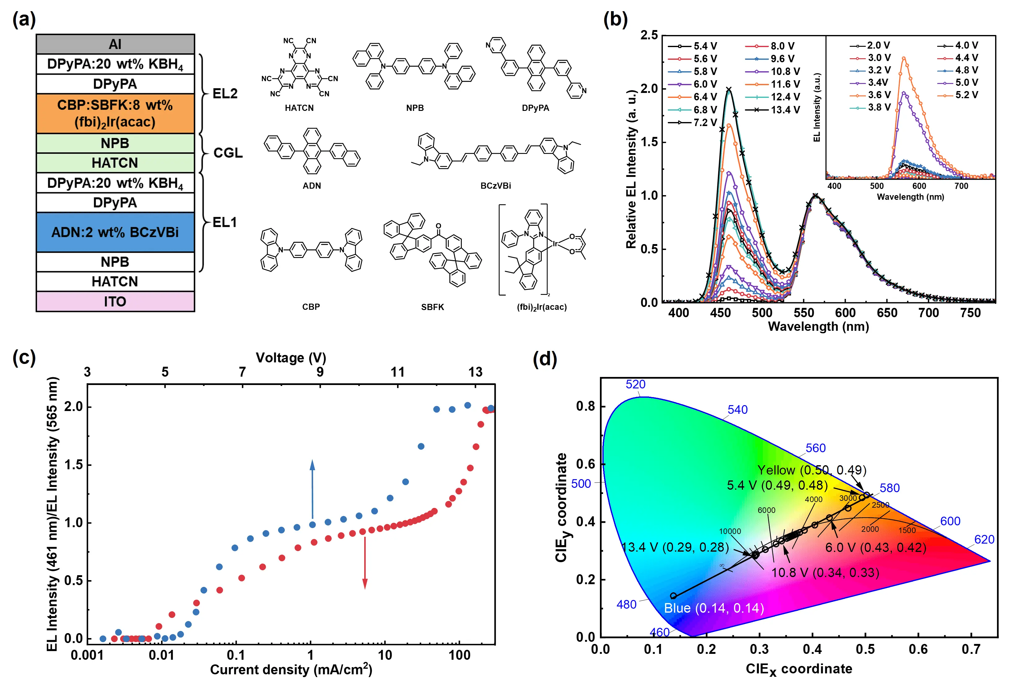
Figure 1. (a) The layer structure of OLED-B, with the molecule structures of the materials used in OLED-B are shown on the right side; (b) EL spectra measured at various applied voltages from 2.0 V to 13.4 V. Zero signal is observed at voltages smaller than 3.4 V, followed by appearance of yellow EL band from 3.4 V, and appearance of the blue EL band above 5.4 V; (c) Intensity ratio of the 461 nm blue emission to the 565 nm yellow emission is plotted against current density (the bottom x axis) and voltage (the top x axis) in OLED-B; (d) CIE chromaticity diagram of tandem OLED-B at various bias voltages between 5.4 V and 13.4 V. Color is changed from reddish white to bluish white with increasing voltage. Color close to the pure white of CIE (0,33, 0.33) is obtained at 10.8 V. EL: electroluminescence; CIE: Commission Internationale de l´Eclairage; OLED: organic light-emitting diodes.
In both EL1 and EL2 units, 9,10-bis(3-(pyridin-3-yl)phenyl)anthracene (DPyPA) is used as ETL, with its high electron mobility of around 10-3 cm2 V-1 s-1, which effectively reduces the electron injection barrier[14]. The layer of DPyPA doped with 20 wt% KBH4 was employed as EIL. The HATCN and NPB are fabricated in sequence after EL1 unit and before EL2 unit to act as CGL. When bias voltage is applied to the device, we expect that HATCN accepts electrons from HOMO level of NPB in CGL and then transport to EIL and ETL of the EL1 unit, while holes are injected from NPB to EL2 unit. After all organic layers are prepared, Al is fabricated as the cathode. The molecule structures of all the organic materials are shown in Figure 1a.
All the organic materials used in OLED fabrication were of sublimation grade purity. Before fabrication, the ITO substrates with a sheet resistance of 15 Ω sq-1 and quartz glass substrates were cleaned and treated with 10-min ozone plasma. All the films were fabricated by thermal evaporation in vacuum chamber at 10-6 Torr onto the substrates and then encapsulated as described previously[29]. During fabrication, quartz crystal sensors are employed to monitor the deposition rates and film thicknesses in situ. The emission area of these three devices is 3 × 3 mm2. Any out-coupling material has not been installed on the ITO surface for all the devices.
The luminance-voltage-current density (L-V-J) characteristics and EL spectra of the OLEDs were measured with a Keithley model 4200 semiconductor characterization system with a calibrated silicon photodiode, and also Konica-Minolta CS-1000 spectroradiometer with a computer controlled programmable Keithley 2400 dc Source Meter. The EQE was measured in an integrated sphere using an integration of a Keithley 2400 source meter and Hamamatsu C9920-12 EQE measurement system, which was equipped with a Hamamatsu PMA-12 photonic multichannel analyzer C10027-02 whose longest detection wavelength is 1,100 nm. The photoluminescence (PL) spectra, photoluminescence excitation (PLE) spectra, and the photovoltaic effect were measured using a Spex Fluoro Max fluorophotometer in a 350-1,000 nm spectral region with a Hamamatsu-Photonics R928 photomultiplier. The excitation was undertaken by illuminating monochromatic light from the 15 W Xe lamp of the Spex Fluoro Max fluorophotometer to OLED-B through its ITO. All measurements were carried out at room temperature.
3. Results and Discussion
3.1 EL performance
Various EL characteristics including advantages and disadvantages are obtained from OLED-B, which are described in detail later. One of the advantages is low driving voltage of 6.5 V at 1,000 cd/m2. Another is the suppressed roll-off.
OLED-B reaches high maximum CE and PE of 60.2 cd/A and 29.6 lm/W at about 1,000 and 350 cd/m2, respectively, which maintain to be 56.4 cd/A and 25.1 lm/W at 10,000 cd/m2, showing a highly suppressed roll-off. With the outstanding charge generation performance of the HATCN/NPB CGL, a much lower driving voltage of 6.5 V at 1,000 cd/m2 is obtained compared with the reference hybrid OLED with MoO3/NPB CGL. The present result provides a promising room light source with its tunable light color through applied voltage and also a display system driven by the low-current operated amorphous Si-TFT (thin film transistor).
The voltage-dependent color change is observed. After the blue emission appearing from 5.4 V, the light color change from warm to cool white is observed during 5.4 V to 13.4 V (Figure 1c,d), and the mechanism well be clarified by analyzing the electronic process inside the device through its energy level diagram later (Section 3.5). Besides, the device also demonstrates photovoltaic effect due to the HATCN/NPB CGL (Section 3.6).
3.2 Characterization of the voltage-dependent color change of the EL spectrum of OLED-B
The EL spectrum of OLED-B consists of a blue BCzVBi emission band and a yellow (fbi)2Ir(acac) emission band. The peak at 461 nm with a vibronic side band at about 489 nm is attributed to the emission of BCzVBi, while the peak at 565 nm with a vibronic side band at about 600 nm belongs to (fbi)2Ir(acac), and the intensity ratio between the blue and yellow bands changes with increasing bias voltage, i.e., current density, as shown in Figure 1b,c. Figure 1c indicates that the blue emission is weaker than the yellow emission at low current density below 10 mA/cm2, the same peak height is obtained at about 22 mA/cm2 (8.0 V), and the blue emission peak becomes higher than the yellow emission band peak at higher current density. The intensity ratio does not change after about 200 mA/cm2 (12.0 V).
The observed voltage-dependent color change is presented by the Commission Internationale de l´Eclairage (CIE) chromaticity coordinate diagram of Figure 1d. The color changes from yellowish warmer white and to bluish cooler white with increasing voltage from 5.4 to 13.4 V. The CIE coordinates (0.34, 0.33) close to the white light coordinates of (0.33, 0.33) are obtained at about 10.8 V, with the correlated color temperature (CCT) of 5,269 K. The CCT and CIE coordinates are 3,165 K and (0.43, 0.42) at 6.0 V, respectively, while they are 9,067 K and (0.29, 0.28) at 13.4 V. The color variation due to change of voltage is useful for lighting, because bluish cooler white is requested in living room in the morning and mid-day, while warmer white is requested in the evening. In the previous studies on the conventional WOLEDs without tandem structure[30], the brightness ratio between the two EL units were not expected to change much with the applied voltage because the current density in each EL unit is equal. The present result, however, reveals the appearance of difference between the blue and yellow-red emission intensities, and leads to a new advantage of tandem OLED.
3.3 Low driving voltage caused by the HATCN/NPB CGL
The luminance-voltage (L-V) and current density-voltage (J-V) characteristics for OLED-B are plotted in Figure 2a. Low driving voltage of 6.5 V (which gives 1.67 mA/cm2) at 1,000 cd/m2 is obtained for OLED-B. For comparison, we examined another white tandem device that was fabricated in a previous work of our group (referred to as OLED-D hereafter), which has the same device structure as OLED-B, except that HATCN was replaced by MoO3[27]. As shown in Figure 2a, much higher driving voltage is obtained for OLED-D than for OLED-B. For example, voltage at 1,000 cd/m2 is 8.7 V (1.47 mA/cm2) for OLED-D. In addition, according to the previous works of white tandem OLEDs with two EL units combined by CGL of Li:BCP/MoO3, Cs2CO3:BCP/MoO3, and Cs2CO3:BPhen/NPB:WO3, luminance of 1,000 cd/m2 was obtained at 14 V[6], 12 V[9], and 8 V[15], respectively, which are all much higher than 6.5 V obtained in OLED-B. Usually, It has been commonly accepted that high driving voltage is an inevitable disadvantage for multi-EL-unit tandem OLEDs[30]. The reason is attributed to larger series resistance due to wide distance between two electrodes in tandem OLED than that in single-stacked OLEDs[31]. The present result obtained from OLED-B, however, denies such a disadvantage for tandem OLEDs since OLED-B shows unusual lower driving voltage than the reference OLED-D, which has the CGL of MoO3. Therefore, it is suggested the driving voltage in tandem OLEDs does not depend on the series resistance but depends on the compositions and structures of CGL.
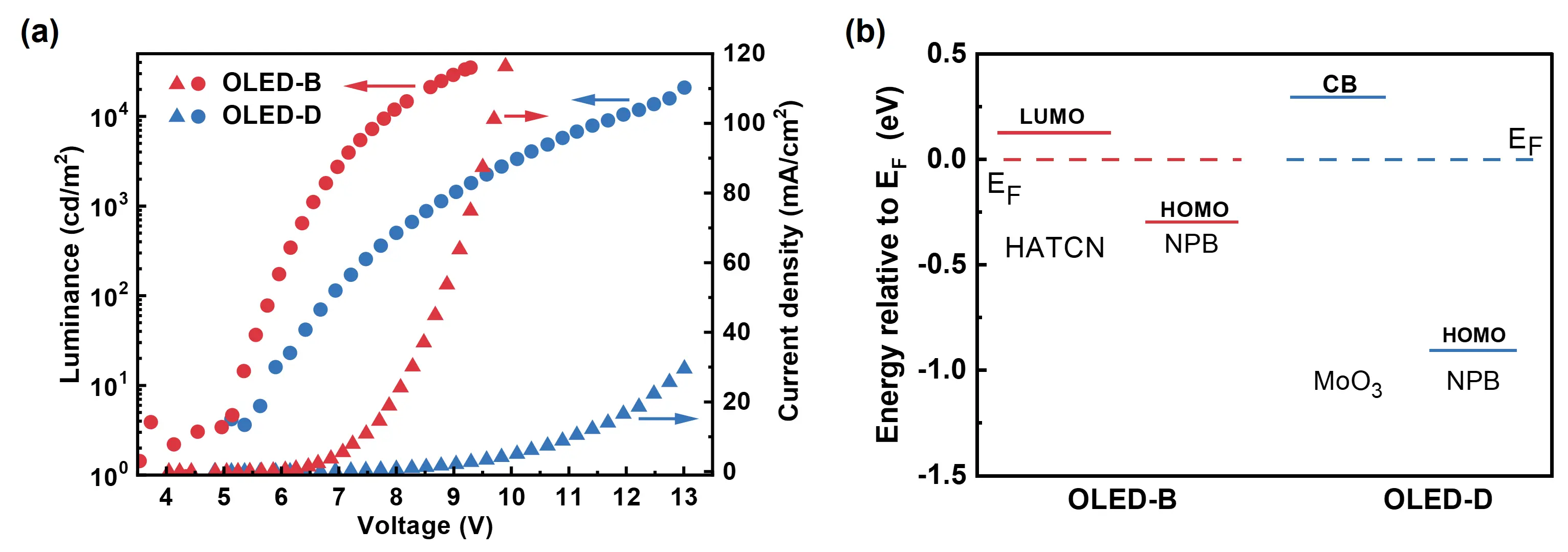
Figure 2. (a) L-V-J characteristics of OLED-B with HATCN/NPB CGL and OLED-D with MoO3/NPB CGL; (b) Energy levels, relative to the Fermi energy (EF), of HATCN and NPB at HATCN/NPB bilayer interface (the left side), and of MoO3 and NPB at MoO3/NPB bilayer interface (the right side), which were determined by ultraviolet photoemission spectroscopy[32,33]. HATCN: 1,4,5,8,9,11-hexaazatriphenylenehexacarbonitrile; NPB: N,N'-di(naphthal-ene-1-yl)-N,N'-diphenylbenzidine; CGL: charge generation layer. L-V-J: luminance-voltage-current density; OLED: organic light-emitting diodes; HOMO: highest occupied molecular orbital; LUMO: lowest unoccupied molecular orbital; CB: conduction band.
To clarify the reason for the low driving voltage of OLED-B, the electronic energy level alignment at the interface between HATCN and NPB has been obtained from previous work with ultraviolet photoemission spectroscopy (UPS) measurement for films of HATCN deposited on NPB[32]. The HOMO level of NPB at the HATCN/NPB interface is located at 0.3 eV below Fermi level, while the LUMO level of HATCN is located at the energy of less than 0.1 eV above the Fermi level. The gap energy between the LUMO of HATCN and the HOMO of NPB near the HATCN/NPB interface is only about 0.4 eV. This energy gap is much narrower than the gap (about 1.3 eV) between the conduction band (CB) of MoO3 and HOMO level of NPB at the MoO3/NPB bilayer interface[33], as shown in Figure 2b. Therefore, the electrons in HOMO of NPB can be more easily injected to LUMO level of HATCN than to CB of MoO3. As a result, much lower driving voltage was obtained for OLED-B than for OLED-D. In conclusion, it is suggested the driving voltage in tandem OLEDs depends on the energy gap between the electron acceptor and donor in CGL.
3.4 High efficiency and low roll-off performance of OLED-B
The current efficiency and power efficiency of OLED-B are plotted against luminance in Figure 3. The maximum CE of 60.2 cd/A and the maximum PE of 29.6 lm/W are obtained at 2,240 cd/m2 (3.72 mA/cm2) and 492 cd/m2 (0.82 mA/cm2), respectively. High current efficiency means that high luminance is achieved at low current density. In fact, we obtained 1,000 cd/m2 at 1.65 mA/cm2 and 10,000 cd/m2 at 17.7 mA/cm2. This indicates a long OLED lifetime because the operation at a lower current density suppresses the device degradation which is caused by Joule heating and polaron-induced quenching processes. For example, in case of OLED-D, LT50 (the time in which the luminance decreases to 50% of its initial value), is obtained to be 800 h and 250 h with the initial luminance of 5,000 cd/m2 and 10,000 cd/m2, respectively.
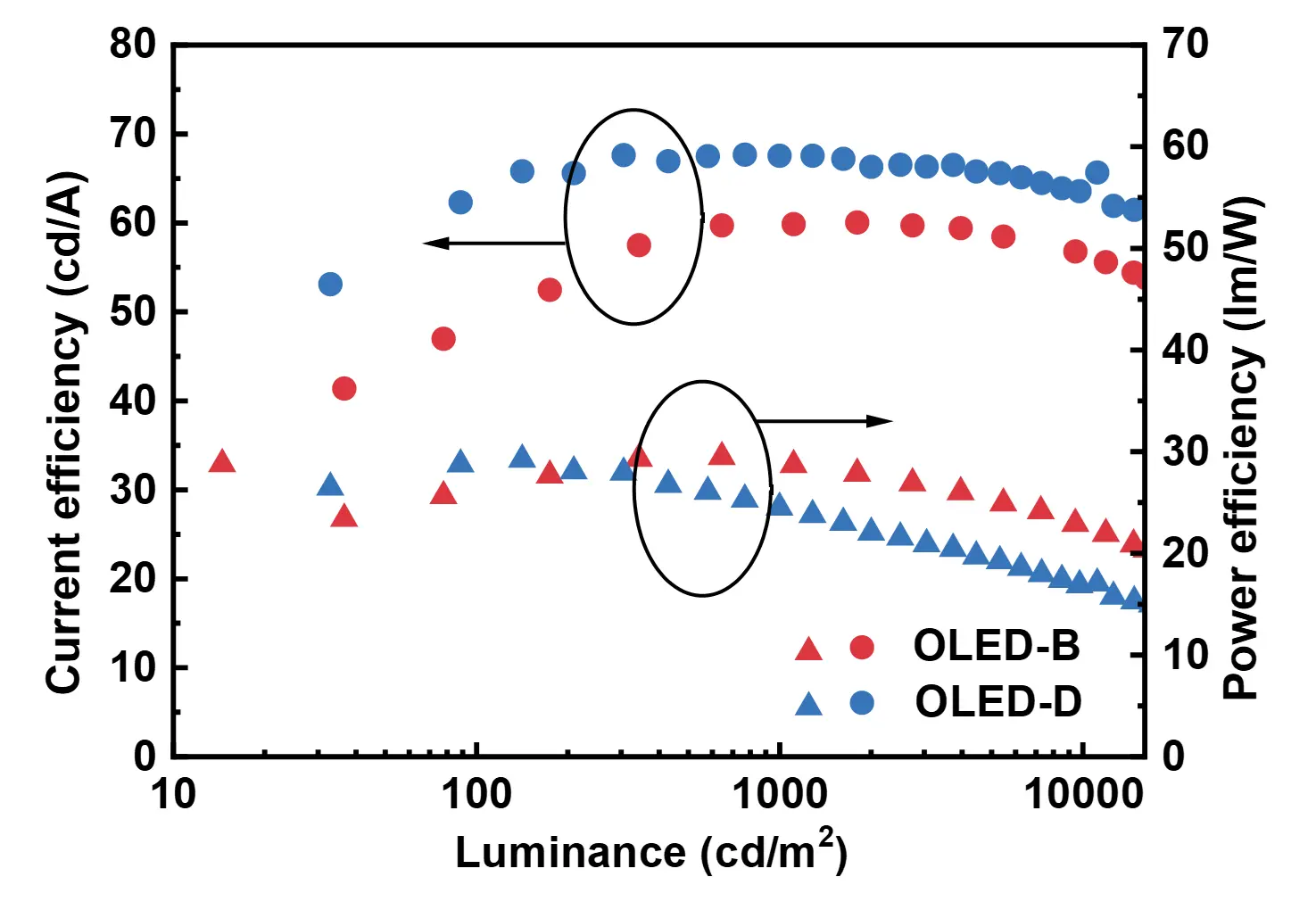
Figure 3. The CE-L and PE-L characteristics of OLED-B with HATCN/NPB CGL and OLED-D with MoO3/NPB CGL. CE-L: current efficiency-luminance; PE-L: power efficiency-luminance; HATCN: 1,4,5,8,9,11-hexaazatriphenylenehexacarbonitrile; NPB: N,N'-di(naphthal-ene-1-yl)-N,N'-diphenylbenzidine; CGL: charge generation layer; OLED: organic light-emitting diodes.
OLED-D shows that the CE (PE) of 68 cd/A (30 lm/W) is obtained at about 1.4 mA/cm2, and 61 cd/A (18 lm/W) at 30 mA/cm2, while they are 60 cd/A (30 lm/W) and 54 cd/A (25 lm/W) for OLED-B at 1.4 mA/cm2 and 30 mA/cm2, respectively. This means that the decrease by 2.5 cd/A (4.0 lm/W) and 2.1 cd/A (1.7 lm/W) is made for the increase by 10 mA/cm2 in OLED-D and OLED-B, respectively. These results suggest that the roll-off leading to device degradation is larger in OLED-D than in OLED-B. A superiority of OLED-B to OLED-D is confirmed from the higher efficiency and smaller roll-off, predicting a longer device lifetime in OLED-B than that in OLED-D.
The superior efficiency performance of OLED-B can be further emphasized by comparison with other hybrid tandem WOLEDs with similar structure. For example, Tyan et al. reported a tandem device, NESD, where EL1 unit has blue fluorescent emitter and EL2 unit has red/yellow phosphorescent emitters[23]. This device, with the same HATCN/NPB CGL and no optical out-coupling structures as OLED-B, showed the luminance of 453 cd/m2, CE of 45.3 cd/A, and PE of 24 lm/W at the current density of 1 mA/cm2, while OLED-B gives higher values of 476 cd/m2, 59.0 cd/A, and 29.6 lm/W, respectively, at the same current density. On the other hand, it has been reported by Chen et al. that the maximum CE is obtained to be 39.2 cd/A at 500 cd/m2 and 29 cd/A at 10,510 cd/m2, which were obtained from a hybrid tandem WOLED with EL1 unit containing blue fluorescent emitter (4,4'-bis(2,28-diphenylvinyl)-1,1'-biphenyl) (DPVBi), and EL2 unit containing yellow phosphorescent emitter (F-BT)2Ir(acac) bis(2-(2-fluorphenyl)-1,3-benzothiozolato-N,C2') iridium (acetylacetonate) [(F-BT)2Ir(acac)], with new type CGL composed of Alq3:Mg/MoO3[34]. This hybrid WOLED is called Device-F hereafter. Compared with Device-F, the OLED-B shows higher CEs of 59.2 cd/A at 500 cd/m2 and 56.2 cd/A at 10,510 cd/m2, respectively. Additionally, it is noteworthy that, despite the same emitters while different CGL containing MoO3 from OLED-B, OLED-D shows 67.5 cd/A at 500 cd/m2 and 63.0 cd/A at 10,510 cd/m2, respectively, whose 5CEs are also higher than those of Device-F. The maximum CE and PE of OLED-D are 68.1 cd/A at 870 cd/m2 (1.28 mA/cm2), and 29.2 lm/W at 141 cd/m2 (0.22 mA/cm2), which are close to those of OLED-B. From these results, the superiority of OLED-B and OLED-D to Device-F is confirmed. One of the reasons may be attributed to the good choice of fluorescence and phosphorescence emitters of BCzVBi and (fbi)2Ir(acac), respectively.
Furthermore, we fabricated another white tandem OLED with the same emitters as OLED-B but the CBP host in EL2 unit is replaced by TCTA host. This OLED is called OLED-G. It exhibits the maximum PE of 25 lm/W and the maximum CE of 70 cd/A, which are close to those (68.1 and 60.2 cd/A) of OLED-D and OLED-B, respectively, providing another evidence for our attribution. The increase from 60.2 cd/A to 70 cd/A by change of host material suggests that influence of the host to the EL performance is not negligible. The PE at 1,000 cd/m2 is 28.8 lm/W for OLED-B while 24.6 lm/W for OLED-D. And it corresponds to 6.5 V for OLED-B while OLED-D, however, needs higher driving voltage of 8.7 V to reach the same luminance of 1,000 cd/m2 (Figure 2a).
This result suggests that HATCN/NPB is more suitable as CGL material than MoO3 although MoO3/NPB is currently used in many tandem OLEDs[6,7,9,21,35,36]. In summary, the excellent combination of fluorescent and phosphorescent emitters guarantees the high efficiency performance, while the HATCN/NPB CGL leads to a low energy consumption for OLED-B.
Such high CEs and PEs of our hybrid tandem WOLED of OLED-B, however, are still much low, compared with the previously reported maximum CE of 110.9 cd/A, PE of 45.2 lm/W, and EQE of 43.3 %, which were obtained from a symmetric tandem white OLED (called PWOLED1) with all-phosphorescence emitters by Wang et al.[6]. In the PWOLED1, a blue emitting EL1 unit with 6.5 wt% FIrpic and a yellow emitting EL2 unit with 0.75 wt% (fbi)2Ir(acac) are connected by the CGL of Li:BCP (10 nm)/MoO3 (7 nm) bilayer. The results are reasonable because OLEDs with all-phosphorescent emitters are expected to exhibit higher efficiencies than the hybrid tandem OLEDs with half fluorescent emitter and half phosphorescent emitter just as the case of OLED-B. Nevertheless, when we examine the reported efficiencies carefully, we find that our efficiencies are not pessimistic. The maximum efficiencies of 110.9 cd/A and 45.2 lm/W were obtained at an extremely low current density of 1 μA/cm2, corresponding to the low luminance of 1.1 cd/m2. Such a very low luminance is not useful in actual application for lighting and display.
When comparing the PEs at 1,000, 2,000, and 10,000 cd/m2 between our and their WOLEDs, the PWOLED1’s efficiencies (estimated from Figure 2 of their paper)[6] are lower than ours, especially much lower at 10,000 cd/m2 as shown in Table 1. This is due to stronger roll-off effect for all-phosphorescence PWOLED1 than for our hybrid WOLED. Consequently, we may conclude that our hybrid tandem OLED is more suitable for lighting and display than PWOLED1 from view of the low roll-off under high luminance. Moreover, OLED-B with pure-organic fluorescent material as blue emitter is expected to have much longer operational lifetime and lower material cost than PWOLED1 with expensive Ir-complex phosphorescent emitters in both EL1 and EL2 units.
Table 1. EL characteristics comparison of OLED-B with Wang et al.’s PWOLED1[6].
| Devices | 1,000 cd/m2 | 2,000 cd/m2 | 10,000 cd/m2 | |||
| PE (lm/W) | CE (cd/A) | PE (lm/W) | CE (cd/A) | PE (lm/W) | CE (cd/A) | |
| OLED-B | 28.8 | 59.9 | 27.5 | 60.1 | 25.1 | 56.4 |
| PWOLED1[6] | 20(a) | 91(a) | 15(a) | 67(a) | 6(a) | 50(a) |
(a) Estimated from Figure 2a; PE: power efficiency; CE: current efficiency; OLED: organic light-emitting diodes; PWOLED: phosphorescent white organic light-emitting diode.
3.5 Mechanism of dual emission of blue and yellow EL bands
As mentioned in Section 3.2, OLED-B demonstrates a voltage-dependent color change of EL spectrum. The blue emission from the EL1 unit never appears at low voltages below 5.2 V although the yellow emission from the EL2 unit starts to appear from about 3.4 V (Figure 1b,c). The blue emission intensity increases with the bias voltage from 5.4 V, and then becomes the same as the yellow emission at 8.0 V (22 mA/cm2), and finally it becomes higher than the yellow emission above this current density (Figure 1c). Here, we examine the reasons why the blue emission does not appear below 5.2 V and why the yellow emission intensity is much higher than the blue emission intensity at low current densities of 0.01-1 mA/cm2 (corresponding to voltages of 5.0-6.4 V) in OLED-B.
In the present CGL with HATCN, the energy gap between the LUMO level of HATCN and the HOMO level of NPB is only about 0.4 eV as mentioned above. Additionally, The HOMO level energy of CBP in EL2 unit is 5.6 eV relative to the vacuum level[37], which is close to the HOMO level of NPB (5.5 eV)[5]. Such an energy level alignment around HOMO level of NPB makes it possible for not only injection of electrons from HOMO level of NPB to HATCN but also transfer of holes from HOMO level of NPB to the adjacent CBP. DPyPA is used as ETL in EL1 unit. However, the LUMO level of DPyPA used as the ETL in EL1 unit is at 2.8 eV[14], which is located at high energy (by 2.7 eV) from the HOMO level of NPB. Such a wide LUMO-HOMO gap between DPyPA and NPB makes the electrons moving from NPB into the EL1 unit impossible at low voltages, leading to difficulty of electron injection into the EL1 unit, even if HATCN layer and KBH4-doped DPyPA layer (as EIL) are inserted between the DPyPA and NPB layers. On the other hand, the electrons are easily injected from the Al cathode to the LUMO level of DPyPA in EL2 unit through EIL when external electrical field is applied, followed by transfer to the LUMO level of SBFK and then (fbi)2Ir(acac) emitter. At the same time, the generated holes in CGL are moved to the HOMO level of (fbi)2Ir(acac) through CBP. Both the electrons and holes are easily injected into the EL2 unit, giving rise to the yellow emission of the EML.
From these results, the following electronic processes are suggested. When the bias voltage applied to OLED-B device is below 5.2 V, holes (open circles in Figure 4a) are easily injected from ITO to NPB in EL1 unit through HATCN layer adjacent to ITO, because HATCN is effective as HIL[13]. The holes then move through the HOMO levels of EL1 unit and arrive at DPyPA layer in EL1 unit, followed by moving to HOMO level of NPB in CGL by the help of HATCN layer in CGL. The holes at NPB are transferred to the HOMO levels of EML in EL2 unit, then recombine with electrons (closed circles in Figure 4a) injected to the LUMO levels of EML in EL2 unit from Al cathode, giving rise to yellow emission from (fbi)2Ir(acac), as illustrated in Figure 4a. The HOMO and LUMO energies and T1 level of CBP are obtained from the work of Schrögel et al.[37], and those of SBFK are obtained from the work of Kondakova et al.[38]. As a result, no blue emission appears from EL1 unit since the electron from HOMO level of NPB in CGL cannot move to LUMO levels of EL1 unit below 5.2 V. This means that HATCN/NPB bilayer does not work as CGL although it was inserted for charge generation. In this way we can explain the reason why only yellow emission appears at low voltages below 5.2 V.
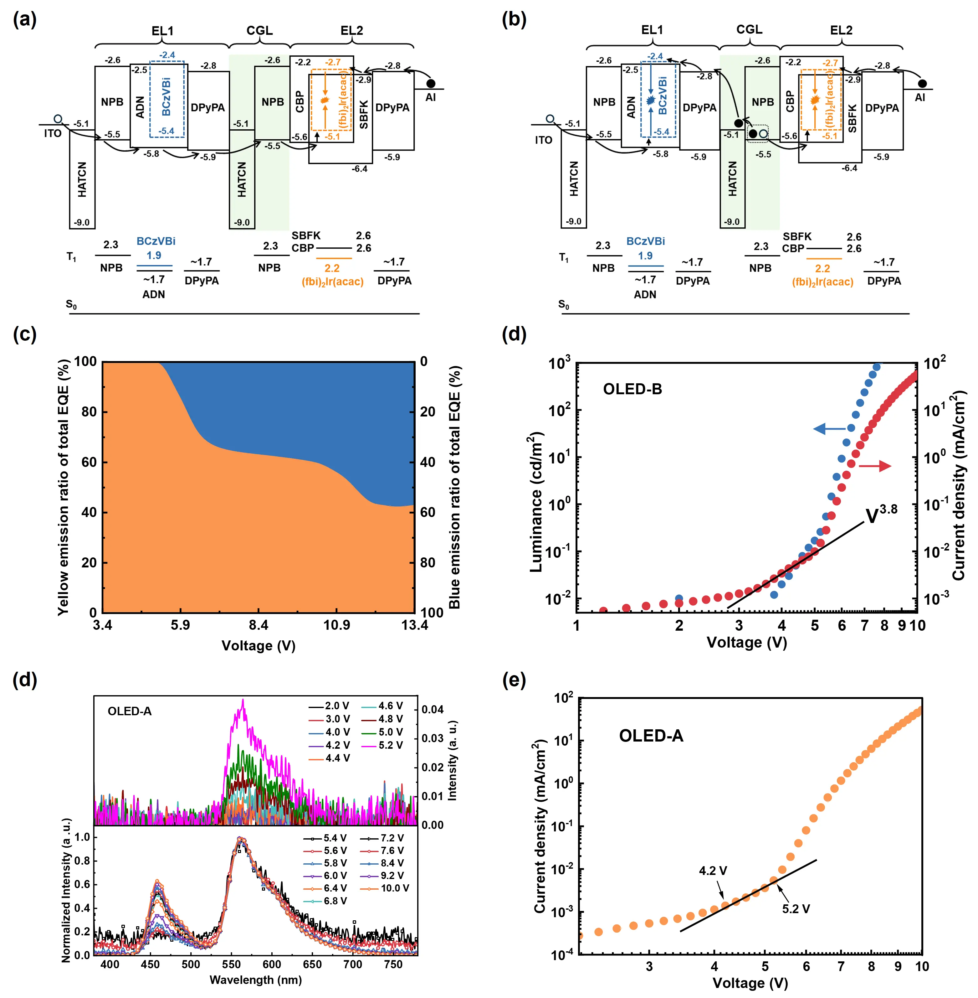
Figure 4. (a) Schematic energy level diagram, drawn relative to the vacuum level, of OLED-B, together with the T1 levels of each material except HATCN and the processes of carrier generation under applied voltages during 3.4 V to 5.2 V, and (b) above 5.4 V; (c) The contribution ratio of the yellow emission band (the orange area, corresponds to the left y axis) and the blue emission band (the blue area, corresponds to the right y axis) to total EQE against voltage; (d) L-V-J characteristics of OLED-B. The blue and yellow emission bands appear above about 5.4 V, while the blue emission does not appear below 5.2 V. The L-V-J characteristics reflect the presence of different electronic processes between 3.4 < V < 5.2 and V > 5.4. A broken straight line is guided by eyes; (e) The EL spectra of OLED-A measured from 2.0 V to 10.0 V. The yellow EL band appears of from 4.2 V, and the blue EL band appears from 5.4 V; (f) The J-V characteristic of OLED-A. The turning point at 4.2 V and 5.4 V agrees with the appearances of yellow EL band and blue EL band, respectively. L-V-J: luminance-voltage-current density; HATCN: 1,4,5,8,9,11-hexaazatriphenylenehexacarbonitrile; EL: electroluminescence; OLED: organic light-emitting diodes.
When the voltage is increased to 5.4 V and higher, electrons (closed circles in Figure 4b) from HOMO level of NPB in CGL begin to move to the LUMO level of DPyPA in EL1 unit through HATCN, then to the LUMO level of BCzVBi by overcoming the electron injection barrier. On the other hand, holes (open circles in Figure 4b) generated in the HOMO state of NPB by moving the electrons to HATCN are transferred to the HOMO level of (fbi)2Ir(acac) in EL2 unit[5,11]. As a result, the blue emission appears from BCzVBi by recombination with holes injected from ITO to HOMO levels of EML in EL1 unit, while there is still yellow emission of (fbi)2Ir(acac), as shown in Figure 4b. Regarding the relative intensity of the yellow and blue emission, it is noteworthy that the efficiency of EL1 with TTA host usually demonstrates an increase initially and then a slow decrease with current density, for the rapid and massive triplet consumption during emitting process, leading to suppressed triplet-induced quenching[39]. In contrast, EL2 with phosphorescence emitter suffers large roll-off due to the long triplet lifetime and slow consumption. As a result, the ratio of the blue photons to the total photons grows and surpasses the yellow emission under high current density, as shown in Figure 4c. Like this, we can explain the reason why the blue emission appears after 5.4 V and its intensity becomes higher than the yellow emission at high voltages above 8.0 V.
A close examination of J-V and L-V characteristics of OLED-B reveals the quite different behaviors between 3.4 < V < 5.2 and V > 5.4 (Figure 4d). The current density J is nearly proportional to V3.8 at 3.4 < V < 5.2 where no blue emission appears, while it increases rapidly above 5.4 V where both the blue and yellow emissions appear with increasing voltage, in proportion to high power of voltage (the power law). The J-V and L-V characteristics confirm the different electronic processes between 3.4 < V < 5.2 and V > 5.4.
In addition, when applied voltage is smaller than 3.4 V, barely EL emission is observed despite weak current. This is understood as follows. At this low voltage, there is no charge generation in CGL because of the high energy gap of about 3 eV between NPB and DPyPA. This means the non-zero current is caused by transport of hole injected from ITO to the HOMO level of NPB in EL1 unit by help of HATCN as a very efficient HIL, followed by sequential transfer through all the HOMO levels of the OLED device and finally moving to the Al cathode, while no electron injects from Al cathode due to the large electron injection barrier. Thus, a hole-only device system is formed at low voltages smaller than 3.4 V.
In summary, electrons in the HOMO level of NPB in CGL cannot be injected into the LUMO level of DPyPA layer in EL1 unit at V < 5.2, because of the wide energy gap. Holes from ITO can be injected to EML in EL2 unit through HOMO levels of EL1 unit and CGL, resulting in yellow emission by recombination with electron injected from Al. Above 5.4 V, electrons in the HOMO level of NPB in CGL are transferred to the LUMO level of HATCN, followed by electron transfer from HOMO levels of EL2 unit to fill the half vacant HOMO level of NPB, resulting in injection of hole into HOMO levels of EML in EL2 unit. The injected holes recombine with electrons injected from Al at (fbi)2Ir(acac) dopants, giving rise to yellow emission. At the same time electrons transferred to LUMO level of HATCN move to the LUMO level of EML in EL1 unit, leading to blue emission by recombination with holes injected from ITO.
The similar phenomenon is also observed in OLED-A, which has the same layer structure as OLED-B except the thickness of NPB used for CGL, where 30 nm thickness of OLED-B is changed to 20 nm in OLED-A, and it showed a maximum EQE of 13.9%. Dual emission is also observed in OLED-A, as seen in Figure 4e. The yellow emission emerges from 4.2 V and the blue emission appears after 5.4 V, and the intensity of the blue emission band is observed to remain smaller than the yellow band in the measured current density range from nearly zero to 55 mA/cm2 (~10 V). The J-V characteristic for OLED-A is shown in Figure 4f. The two turning points of 4.2 V and 5.2 V are in basically consistent with the appearances of yellow and blue emissions. This is another evidence for the mechanism raise above.
3.6 Photovoltaic effect
Figure 5a shows the PL spectrum of OLED-B, which was obtained by illuminating the monochromatic light of 330 nm to the device through ITO. The PL spectrum at 430-520 nm is attributed to BCzVBi from comparison with the PL spectrum of BCzVBi[40], while the PL spectrum at 540-700 nm is attributed to (fbi)2Ir(acac) from comparison with PL spectrum of (fbi)2Ir(acac)[6]. The PLE spectrum for 450 nm consists of an intense band with a peak at 360 nm and a weak band at about 400 nm. The 400 nm band is attributed to BCzVBi from the absorption spectrum of BCzVBi[40], while the intense 360 nm band is attributed to NPB. These PL and PLE spectra of OLED-B confirm that both (fbi)2Ir(acac) and BCzVBi molecules are present stably in the multi-layered device even after long device operation time.
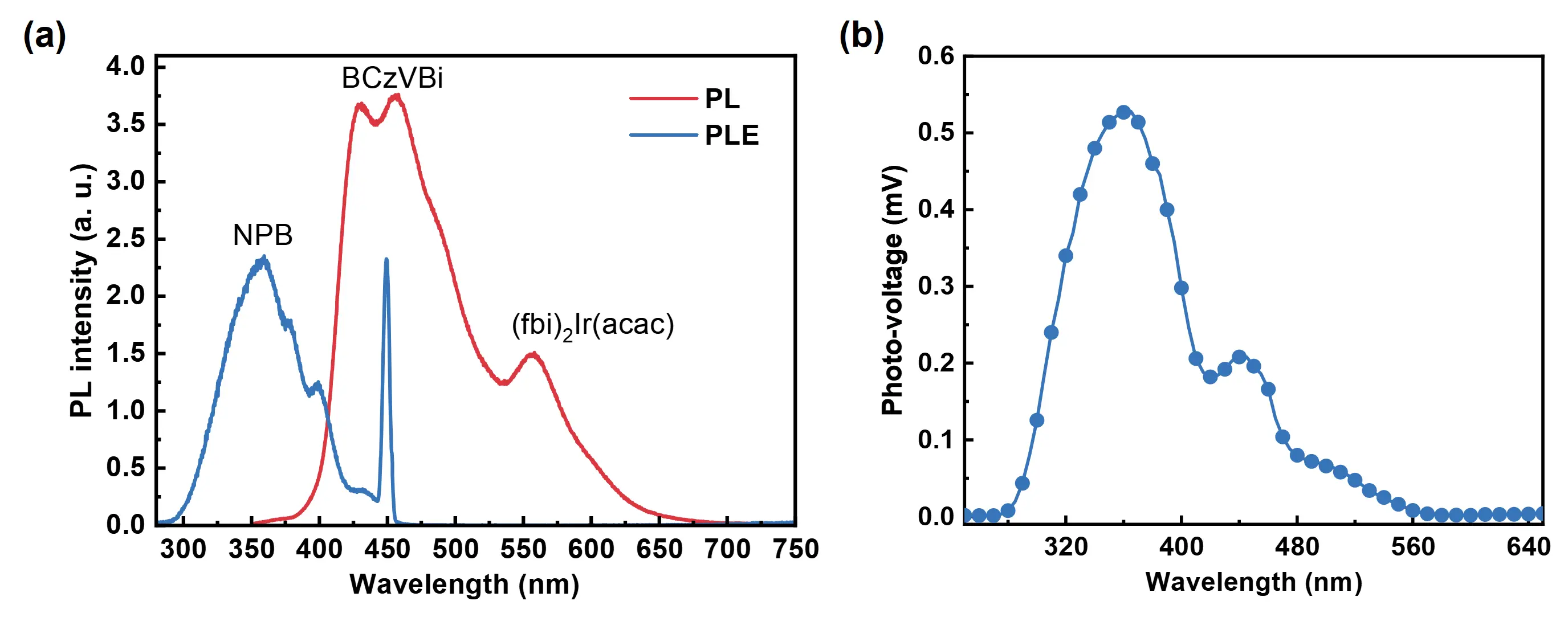
Figure 5. (a) PL spectrum of OLED-B excited at 330 nm and PLE spectrum for 450 nm emission. A sharp peak at 450 nm is due to the excitation light from Xe-lamp source; (b) Photo-voltage spectrum of OLED-B. NPB: N,N'-di(naphthal-ene-1-yl)-N,N'-diphenylbenzidine; PL: photoluminescence; PLE: photoluminescence excitation; OLED: organic light-emitting diodes.
The photoexcitation into OLED-B was found to generate a voltage in the device with negative charge at the Al metal and positive charge at ITO. The photo-voltage of OLED-B is plotted against the wavelength of illuminating light to this device in Figure 5b. Intense photovoltage appears at about 360, 440, and 500 nm. The last two bands are attributable to (fbi)2Ir(acac) from comparison with the absorption spectrum of (fbi)2Ir(acac)[6]. The 360 nm band is attributed to NPB from comparison with PLE spectrum of Figure 5a. The observed photovoltaic effect is explained as follows.
Photoexcitation into NPB generates electrons in the LUMO level of NPB, followed by moving into the LUMO level of EL2 unit and into Al cathode, leading to accumulation of electrons at Al. Simultaneously, holes are generated in the HOMO level of NPB, followed by moving into the HOMO level of EL1 unit through HATCN layer, and finally into ITO, leading to accumulation of holes at ITO. As a result, the photo-voltage (PV) is generated in OLED-B. The same electronic processes occur for the photo-excited (fbi)2Ir(acac). The observed photo-voltaic effect indicates that (1) the HATCN layer used in CGL makes the holes transfer from NPB into the EL1 unit easy, and (2) the energy level diagram of Figure 4a,b is reasonable.
3.7 Comparisons of the EL performance among five WOLEDs
Table 2 summarizes the maximum CEs, PEs and the driving voltages required to achieve a luminance of 1,000 cd/m2 for use as an actually employed lighting device, which are obtained from hybrid tandem WOLEDs by our group in this study and previous works. It could be noticed that both devices with MoO3/NPB CGL exhibited the driving voltages higher than 8 V. Specifically, OLED-D, which shares the same EL units with OLED-B and OLED-A but utilizes a MoO3/NPB CGL, demonstrated the highest driving voltage of 8.7 V at 1,000 cd/m², along with the highest CE of 60.2 cd/A. The driving voltage was increased from 6.5 V to 7.3 V after the thickness of NPB used for CGL was changed from 30 nm of OLED-B to 20 nm of OLED-A, while keeping other structures the same as OLED-B. However, it is still lower than that of OLED-D. These results clarified that the choice of materials and thickness used for CGL had great impact on the performance of tandem WOLEDs. In addition, by switching EL2-2 of OLED-B to EL2-3, OLED-G obtained higher CE of 70 cd/A but sharply increased driving voltage of 8.8 V and deceased PE of 25 lm/W. Also, in Section 3.4 we compared the OLED-B and PWOLED-1, and concluded the superiority of OLED-B with hybrid device structures. These results indicated the choice of EML materials for EL1 and EL2 units also contributed to the device performance. Though the maximum current efficiency of OLED-B does not rank the top, it is still the preferable hybrid WOLED for the lowest driving voltage of 6.5 V at the luminance of 1,000 cd/m2 (corresponding to current density of 1.67 mA/cm2), together with the highest maximum power efficiency of 29.6 lm/W.
Table 2. Examples of EL performance, including the Max CE and the Max PE, and DV generating luminance of 1,000 cd/m2 observed from several hybrid tandem WOLEDs, together with the whole layer structure, layer structures of EL1 and EL2 unit and CGL.
| WOLED | Whole layer structure | EL1 unit | CGL | EL2 unit | Max CE (cd/A) | Max PE (lm/W) | DV for 1,000cd/m2 (V) | Ref. |
| WOLED1 | A1 | EL1-1 | MoO3 (10 nm)/NPB (40 nm) | EL2-1 | 75 | NA | 8.4 | [26] |
| WOLED2 (OLED-D) | A2 | EL1-2 | MoO3 (10 nm)/NPB (30 nm) | EL2-2 | 68.1 | 29.2 | 8.7 | [27] |
| WOLED3-1 (OLED-B) | A3-1 | EL1-2 | HATCN (10 nm)/NPB (30 nm) | EL2-2 | 60.2 | 29.6 | 6.5 | Present study |
| WOLED3-2 (OLED-G) | A3-1 | EL1-2 | HATCN (10 nm)/NPB (30 nm) | EL2-3 | 70 | 25 | 8.8 | |
| WOLED3-3 (OLED-A) | A3-2 | EL1-2 | HATCN (10 nm)/NPB (20 nm) | EL2-2 | 58.7 | 25.3 | 7.3 |
A1: ITO/MoO3 (20 nm)/EL1/MoO3 (10 nm)/NPB (40 nm)/EL2/Al; A2: ITO/MoO3 (10 nm)/EL1/MoO3 (10 nm)/NPB (30 nm)/EL2/Al; A3-1: ITO/HATCN (10 nm)/EL1/HATCN (10 nm)/NPB (30 nm)/EL2/Al; A3-2: ITO/HATCN (10 nm)/EL1/HATCN (10 nm)/NPB (20 nm)/EL2/Al; EL1-1: NPB (20 nm)/ADN: 5wt% BCzVBi (10 nm)/DPyPA:20wt% KBH4 (20 nm); EL1-2: NPB (30 nm)/ADN: 2wt% BCzVBi (30 nm)/DPyPA (10 nm)/DPyPA:20wt% KBH4 (20 nm); EL2-1: TCTA:SBFK (1:1):13wt% (fbi)2Ir(acac) (30 nm)/SBFK (5 nm)/DPyPA (20 nm)/DPyPA: 20wt% KBH4 (25 nm); EL2-2: CBP:SBFK (1:1): 8wt% (fbi)2Ir(acac) (30 nm)/DPyPA (10 nm)/DPyPA:20wt% KBH4 (20 nm); EL2-3: TCTA:SBFK (1:1):8 wt% (fbi)2Ir(acac) (30 nm)/DPyPA (10 nm)/DPyPA:20 wt%KBH4 (20 nm); NPB: N,N'-di(naphthal-ene-1-yl)-N,N'-diphenylbenzidine; EL: electroluminescence; OLED: organic light-emitting diodes; Max CE: maximum current efficiency; Max PE: maximum power efficiency; DV: driving voltage; WOLEDs: white organic light-emitting diodes; CGL: charge generation layer.
4. Conclusion
Tandem WOLEDs have been expected to achieve low-energy consumption device giving high luminance at low-voltage operation. The actual EL performance of the driving voltage and the maximum current and power efficiencies, however, does not satisfy the expectation. In the present study, the lowest driving voltage of 6.5 V at 1,000 cd/m2 is achieved from hybrid OLED-B with a CGL of HATCN (10nm)/NPB (30nm), together with high maximum PE of 29.6 lm/W and CE of 60.2 cd/A. Switching the NPB thickness from 30 nm to 20 nm keeping other structures unchanged gives slightly dropped CE and PE with a rising driving voltage of 7.3 V for OLED-A, which is still lower than the 8.7 V of OLED-D with MoO3/NPB CGL. The low driving voltage comes from the small LUMO-HOMO gap of 0.4 eV at HATCN/NPB interface. Similar driving voltage rise and PE drop are observed by changing the mixed host of CBP:SBFK (1:1) in OLED-B to TCTA:SBFK (1:1) in OLED-G. In addition, OLED-B also demonstrates superiority over all-phosphorescence WOLEDs like PWOLED-1 in roll-off and operational lifetime, for its hybrid EMLs with blue fluorescent emitter and yellow phosphorescent emitter. Like this, the excellent EL performance is revealed to largely depend on the elaborate combination of not only the component and layer thickness of CGL, but also the choices of EML materials. The OLED-B only emits yellow emission at low voltages below 5.2 V, while blue-yellow dual emissions from 5.4 V to 13.4 V, which could be reasonable interpreted by the different function of HATCN layer in the electronic process inside CGL during the two voltage-range. This mechanism also generates voltage-dependent spectrum from yellowish white to bluish white with increasing voltage from 5.4 V to 13.4 V, which is useful for lighting in the living room. Our work here offers a practical strategy to fabricate WOLED with high efficiency and low driving voltage, and it is promising in the application of WOLED-light field.
Acknowledgements
Taiju Tsuboi acknowledges a research support of Zhejiang University.
Authors contribution
Li X: Made the devices, analyzed the experiment data.
Tsuboi T: Carried out the spectra measurements, analyzed the experiment data, jointly conceived and supervised the project.
Duan L: Jointly conceived and supervised the project.
All authors discussed the results and wrote the manuscript.
Conflicts of interest
The authors declare no conflicts of interest.
Ethical approval
Not applicable.
Consent to participate
Not applicable.
Consent for publication
Not applicable.
Availability of data and materials
The data and materials could be obtained from the corresponding author upon reasonable request.
Funding
This research was financed by the National Key Research and Development Program (Grant Nos. 2020YFA0715002 and 2021YFB3602702), the National Natural Science Foundation of China (Grant Nos. 52222308, 22135004 and 61890942), the Guangdong Basic and Applied Basic Research Foundation (Grant No. 2021B1515120041) and the Guangdong Major Project of Basic and Applied Basic Research (Grant No. 2019B030302009).
Copyright
© The Author(s) 2025.
References
-
1. Tang CW, Vanslyke SA. Organic electroluminescent diodes. Appl Phys Lett. 1987;51(12):913-915.[DOI]
-
2. Fung MK, Li YQ, Liao LS. Tandem organic light-emitting diodes. Adv Mater. 2016;28(47):10381-10408.[DOI]
-
3. Huang C, Zhang Y, Zhou J, Sun S, Luo W, He W, et al. Hybrid tandem white OLED with long lifetime and 150 lm W-1 in luminous efficacy based on TADF blue emitter stabilized with phosphorescent red emitter. Adv Optical Mater. 2020;8(18):2000727.[DOI]
-
4. Xie YM, Liao LS, Fung MK. Hybrid design of light-emitting diodes in tandem structures. Adv Funct Mater. 2025;35(21):2401789.[DOI]
-
5. Chiba T, Pu YJ, Miyazaki R, Nakayama K, Sasabe H, Kido J. Ultra-high efficiency by multiple emission from stacked organic light-emitting devices. Org Electron. 2011;12(4):710-715.[DOI]
-
6. Wang Q, Ding J, Zhang Z, Ma D, Cheng Y, Wang L, et al. A high-performance tandem white organic light-emitting diode combining highly effective white-units and their interconnection layer. J Appl Phys. 2009;105(7):076101.[DOI]
-
7. Guo F, Ma D. White organic light-emitting diodes based on tandem structures. Appl Phys Lett. 2005;87(17):173510.[DOI]
-
8. Zhang H, Su Q, and Chen S. Quantum-dot and organic hybrid tandem light-emitting diodes with multi-functionality of full-color-tunability and white-light-emission. Nat Commun. 2020;11(1):2826.[DOI]
-
9. Lee TW, Noh T, Choi BK, Kim MS, Shin DW, Kido J. High-efficiency stacked white organic light-emitting diodes. Appl Phys Lett. 2008;92(4):043301.[DOI]
-
10. Wang J, Wang Y, Qin Y, Li R, An J, Chen Y, et al. Highly efficient ultra-flexible tandem organic light-emitting diodes adopting a non-doped charge generation unit. J Mater Chem C.2021;9(27):8570-8578.[DOI]
-
11. Park SM, Kim YH, Yi Y, Oh HY, Kim JW. Insertion of an organic interlayer for hole current enhancement in inverted organic light emitting devices. Appl Phys Lett. 2010;97(6):0633081.[DOI]
-
12. Liu Z, Wei P, Bin Z, Wang X, Zhang D, Lian D. Approaching ohmic hole contact via a synergetic effect of a thin insulating layer and strong electron acceptors. Sci China Mater. 2021;64(12):3124-3130.[DOI]
-
13. Li S, Sun W, Li X, Xia X, Zhou L. Low operation voltage white organic light-emitting diodes with excellent color stability based on gradient-doping sensitization system. Adv Opt Mater. 2023;11(5):2202472.[DOI]
-
14. Sun Y, Duan L, Zhang D, Qiao J, Dong G, Wang L, et al. A pyridine-containing anthracene derivative with high electron and hole mobilities for highly efficient and stable fluorescent organic light-emitting diodes. Adv Funct Mater. 2011;21(10):1881-1886.[DOI]
-
15. Ho MH, Chen TM, Yeh PC, Hwang SW, Chen CH. Highly efficient p-i-n white organic light emitting devices with tandem structure. Appl Phys Lett. 2007;91(23):233507.[DOI]
-
16. Xie X, Hu X, Qin Y, Shen S, Dong X, Pang Z, et al. Stable all-fluorescence white organic light-emitting diodes with high efficiency and high CRI. Adv Opt Mater. 2024;12(20):2400441.[DOI]
-
17. Chiba T, Pu YJ, Kido J. Solution-processed white phosphorescent tandem organic light-emitting devices. Adv Mater. 2015;27(32):4681-4687.[DOI]
-
18. Miao YQ, Wei XZ, Gao L, Wang KX, Zhao B, Wang ZQ, et al. Tandem white organic light-emitting diodes stacked with two symmetrical emitting units simultaneously achieving superior efficiency/cri/color stability. Nanophotonics. 2019;8(10):1783-1794.[DOI]
-
19. Du C, Liu H, Cheng Z, Zhang S, Qu Z, Yang D, et al. Ultraefficient non-doped deep blue fluorescent OLED: Achieving a high EQE of 10.17% at 1,000 cd m-2 with CIEy < 0.08. Adv Funct Mater. 2023;33(45):2304854.[DOI]
-
20. Lee K H, Jo U, Kim JM, Lee JY. Role of tailoring exciplex-forming cohosts in the longevity of blue phosphorescent organic light-emitting diodes. Adv Funct Mater. 2024;34(39):2402963.[DOI]
-
21. Kanno H, Giebink N C, Sun Y, Forrest SR. Stacked white organic light-emitting devices based on a combination of fluorescent and phosphorescent emitters. Appl Phys Lett. 2006;89(2):023503.[DOI]
-
22. Liao LS, Ren X, Begley WJ, Tyan YS, Pellow CA. 54.2: Tandem white OLEDs combining fluorescent and phosphorescent emission. SID Symp Dig Tech Papers. 2008;39(1):818-821.[DOI]
-
23. Tyan YS, Rao YQ, Ren XF, Kesel R, Cushman TR, Beglry WJ, et al. 60.1: Invited paper: Tandem hybrid white OLED devices with improved light extraction. SID Symp Dig Tech Papers. 2009;40(1):895-898.[DOI]
-
24. Hatwar TK, Spindler JP, Kondakova M Giesen D, Deaton J, Vargas JR. 52.2: Hybrid tandem white OLEDs with high efficiency and long life-time for AMOLED displays and solid-state lighting. SID Symp Dig Tech Papers. 2010;41(1):778-781.[DOI]
-
25. Zhu G, Fan Q, Hu T, Han YQ, Zhang GS, Zou JH, et al. Largely improving the lifetime by inserting a Yb metal layer into the charge generation layer in tandem organic light-emitting diodes. Org Electron. 2023;122:106908.[DOI]
-
26. Duan L, Tsuboi T, Qiu Y, Li Y, Zhang G. Tandem organic light-emitting diodes with KBH4 doped 9,10-bis(3-(pyridin-3-yl)phenyl) anthracene connected to the charge generation layer. Opt Express. 2012;20(13):14564-14572.[DOI]
-
27. Duan L, Tsuboi T, Qiu Y. Highly efficient hybrid white tandem organic light-emitting diodes with MoO3 layer. Chin J Chem. 2015;33(8):859-864.[DOI]
-
28. Shi W, Yue Y, Zhao B, Xu H, Cao C, Lan W, et al. Effect of the glass transition temperature of organic materials on exciton recombination region of deep blue oled under thermal stress. Adv Eng Mater. 2024;26(5):2301584.[DOI]
-
29. Liu Z, Li X, Lu Y, Zhang C, Zhang Y, Huang T, et al. In situ-formed tetrahedrally coordinated double-helical metal complexes for improved coordination-activated n-doping. Nat Commun. 2022;13(1):1215.[DOI]
-
30. Gather MC, Köhnen A, Meerholz K. White organic light-emitting diodes. Adv Mater. 2011;23(2):233-248.[DOI]
-
31. Lai SL, Chan MY, Fung MK, Lee CS, Lee ST. Copper hexadecafluorophthalocyanine and copper phthalocyanine as a pure organic connecting unit in blue tandem organic light-emitting devices. J Appl Phys. 2007;101(1):014509.[DOI]
-
32. Wei H, Zhang R, Huang G, Yuan Y, Chen W. Interfacial charge transfer study of hexacarbonitrile-based intermediate connecter in blue tandem organic light-emitting diodes. Opt Mater. 2022;128:112345.[DOI]
-
33. Meng SG, Zhu XZ, Zhou DY, Laio LS. Recent progresses in solution-processed tandem organic and quantum dots light-emitting diodes. Molecules. 2023;28(1):134.[DOI]
-
34. Chen P, Xue Q, Xie W, Duan Y, Zhao Y, Liu S, et al. Influence of interlayer on the performance of stacked white organic light-emitting devices. Appl Phys Lett. 2009;95(12):123307.[DOI]
-
35. Li R, Wang J, Qin Y, Liu C, Wang Y, Zhang X, et al. Inverted organic light-emitting devices using a charge-generation unit as an electron injector. Org Electron. 2020;76:105445.[DOI]
-
36. Park Y, Choi HR, Jeon Y, Kin H, Shin JW, Huh CH, et al. Cell proliferation effect of deep-penetrating microcavity tandem NIR OLEDs with therapeutic trend analysis. Sci Rep. 2022;12(1):10935.[DOI]
-
37. Schrögel P, Tomkevičienė A, Strohriegl P, Hoffmann ST, Köhler A, Lennartz C. A series of CBP-derivatives as host materials for blue phosphorescent organic light-emitting diodes. J Mater Chem. 2011;21(7):2266-2273.[DOI]
-
38. Kondakova ME, Pawlik TD, Young RH, Geesen DJ, Kondakov DY, Brown CT, et al. High-efficiency, low-voltage phosphorescent organic light-emitting diode devices with mixed host. J Appl Phys. 2008;104(9):094501.[DOI]
-
39. Cao C, Yang GX, Tan JH, Shen D, Chen WC, Chen JX, et al. Deep-blue high-efficiency triplet-triplet annihilation organic light-emitting diodes using donor-and acceptor-modified anthracene fluorescent emitters. Mater Today Energy. 2021;21:100727.[DOI]
-
40. Jung ED, Kim CU, Noh YW, Seo SK, Noh YI, Choi KJ. Aesthetic and efficient perovskite/si tandem solar cells using luminescent down-shifting textured anti-reflection films. EcoMat. 2023;5(10):e12399.[DOI]
Copyright
© The Author(s) 2025. This is an Open Access article licensed under a Creative Commons Attribution 4.0 International License (https://creativecommons.org/licenses/by/4.0/), which permits unrestricted use, sharing, adaptation, distribution and reproduction in any medium or format, for any purpose, even commercially, as long as you give appropriate credit to the original author(s) and the source, provide a link to the Creative Commons license, and indicate if changes were made.
Publisher’s Note
Science Exploration remains a neutral stance on jurisdictional claims in published
maps
and institutional affiliations. The views expressed in this article are solely those
of
the author(s) and do not reflect the opinions of the Editors or the publisher.
Share And Cite


Science Exploration Style
Li X, Tsuboi T, Duan L. Highly efficient hybrid tandem white organic light-emitting diodes with two different color-emitting units. Smart Mater Devices. 2025;1:36716. https://doi.org/10.70401/smd.2025.0003
Tips
Copy completed.
Submit a Manuscript
Author Instructions
Cite this Article
Article Metrics
0
View
0
Download
Cited
Article Updates

Science Exploration Style
Li X, Tsuboi T, Duan L. Highly efficient hybrid tandem white organic light-emitting diodes with two different color-emitting units. Smart Mater Devices. 2025;1:36716. https://doi.org/10.70401/smd.2025.0003
copy
Share Link
copy