Ultra-thin spray cooling for high-power-density silicon chips
Rui Zhou

Yitao Shen
Jindong Yan
Hua Chen
*
,
Wen-Long Cheng
*
*Correspondence to:
Hua Chen, Department of Thermal Science and Energy Engineering, University of Science and Technology of China, Hefei 230027, Anhui, China.
E-mail: huami@ustc.edu.cn
Wen-long Cheng, Department of Thermal Science and Energy Engineering, University of Science and Technology of China, Hefei 230027, Anhui, China. E-mail: wlcheng@ustc.edu.cn
Wen-long Cheng, Department of Thermal Science and Energy Engineering, University of Science and Technology of China, Hefei 230027, Anhui, China. E-mail: wlcheng@ustc.edu.cn
Thermo-X. 2026;2:202603. 10.70401/tx.2026.0014
Received: January 19, 2026Accepted: March 04, 2026Published: March 09, 2026
Abstract
Driven by the escalating chip-level heat flux demands of artificial intelligence and high-performance computing, thermal management has emerged as a critical bottleneck for next-generation microelectronic integration. To address the prominent contradiction between the limited space and the high heat flux in silicon interconnect fabric chips, this research has overcome the key challenge of miniaturizing traditional spray cooling by designing and implementing an ultra-thin spray cooling heat sink embedded in a silicon-based test chip. The core advancement stems from a synergistic integration of topology-optimized micro-nozzle architecture and silicon-based microfabrication, achieving a total spray module thickness of merely 3.5 mm and enabling uniform near-field atomization from four nozzles under low pressure. Experimental results demonstrate that the heat sink removes 614 W at a junction temperature of 92 °C from a compact footprint of 9.5 mm × 9.5 mm, yielding a peak surface heat transfer coefficient of 9.03 W/(cm2·K). This performance not only validates the feasibility of spray cooling in ultra-thin packaging architectures, but also presents one of the first experimental demonstration of the monolithic integration of a spray cooling system with a silicon-based integrated circuit. This work establishes a viable pathway for ultra-high heat flux thermal management under extreme spatial constraints, enabling the practical deployment of spray cooling in high-power-density electronics, including high-performance computing and artificial intelligence chips.
Graphical Abstract
Keywords
Ultra thin, spray cooling, silicon interconnect fabric chips, thermal management
1. Introduction
The advent of array chips packaged via Silicon Interconnect Fabric (Si-IF) has revolutionized conventional chip packaging paradigms. By integrating silicon wafers with multiple bare chips[1-3], this technology eliminates the limitations imposed by printed circuit boards (PCBs), enabling signal transmission with higher bandwidth and lower power loss[4]. It is anticipated to overcome the bottlenecks of Moore’s Law and assume a pivotal role in future high-performance computing[5]. In the global landscape of high-performance AI computing, leading-edge products, such as Tesla’s Dojo wafer chip (featuring a 5 × 5 array with a total power rating of 15 kW)[6] and Cerebras’ WSE-3 wafer-level chip (incorporating a 7 × 12 array on a 12-inch substrate, with a total power consumption of 17.6 kW)[7], uniformly adopt Si-IF packaging to deliver state-of-the-art performance metrics. Nevertheless, it is critical to note that approximately 50% of electronic device failures occur when temperatures reach 75 °C, which is attributed to thermal load-induced stress[8-10]. While enabling higher integration and increased power density, Si-IF array chips are concurrently confronted with more critical thermal failure challenges. This is primarily attributed to the smooth substrate of Si-IF array chips, which lacks dedicated thermal spreading structures, leading to a substantially higher actual heat flux density than that of conventional semiconductors. When subjected to high heat flux impingement, such chips are susceptible to multiple failure modes, including the degradation of copper pillar interconnects between the silicon substrate and bare chips[11,12]. Accordingly, the exploration of high-performance, highly integrated thermal management technologies tailored to Si-IF array chips is of critical importance.
Among advanced thermal management techniques, microchannel cooling and spray cooling stand out as two of the most actively pursued approaches by both the scientific community and leading research institutions[13,14]. A key commonality between these two approaches lies in their utilization of fluid miniaturization to enable short-path heat transfer, which suppresses the growth and thickening of thermal boundary layers—thereby achieving ultra-high heat fluxes of up to 3,190 W/cm2[15] and convective heat transfer coefficients of 443.7 kW/(m2·K)[16].
Specifically, as an enhanced heat transfer technique characterized by high-pressure impingement, low fluid consumption, and efficient utilization of phase-change latent heat, spray cooling exhibits exceptional thermal management potential in space-constrained environments[17]. Its core operating mechanism is as follows: Pressurized cooling medium is atomized via nozzles to form microscale droplets, which achieve the objective of fluid miniaturization. These droplets impinge on high-heat-flux surfaces, disrupting the developing thermal boundary layer and generating abundant vaporization nucleation sites, thus enabling efficient heat removal[18-20]. In 2020, Opoku et al. demonstrated a critical heat flux of 225 W/cm2 under a low flow rate of 1.26 mL/s using deionized water[21]; in 2024, Zhou et al. demonstrated a heat transfer performance of 435 W/cm2 near the boiling point of the working fluid via a single nozzle[22]; subsequently, they further enhanced the heat transfer capacity to 522 W/cm2 in follow-up studies[23]. In 2025, Hu et al. optimized evaporation and liquid film boiling behaviors on three-dimensional (3D) ordered hierarchical micro/nanostructured surfaces, achieving a heat flux of 1,273 W/cm2 and a heat transfer coefficient of 443.7 kW/(m2·K). This work demonstrates the substantial potential of spray cooling for high-performance thermal management[16].
Although spray cooling exhibits exceptional heat transfer performance, its integration into chip-scale thermal management has been fundamentally hindered by persistent challenges in system miniaturization and on-die integration. To overcome these barriers, recent efforts have focused on aggressive footprint reduction, enabling not only device-level integration but also direct incorporation into monolithic chip thermal management architectures. In 2019, Jiang et al. proposed a compact spray cooling module integrated with 8 nozzles, featuring an overall footprint of 380 × 80 × 10 mm and achieving a heat flux of 304.7 W/cm2[24]. In 2023, Carneiro et al. fabricated a compact spray cooling heat sink, which achieved a heat dissipation capacity of 230 W and maintained the heater surface temperature below 22.9 °C[25]. In 2024 and 2025, Fu, Zhou, et al. integrated a spray array consisting of 60 micro-nozzles into a cold plate with a thickness of merely 16 mm. Utilizing R134a as the working fluid, they achieved a vaporization rate of 52.1%, which provides valuable insights for the further compact design of spray cooling heat sinks[26,27].
However, existing studies have primarily emphasized the dimensional miniaturization of the spray system, without resolving the core integration challenges associated with Si-IF chip substrates. Realizing seamless integration, therefore, requires high-precision micro/nanofabrication techniques that are fully compatible with silicon semiconductor manufacturing processes. In this context, advances in microchannel heat sink technology offer instructive parallels for spray cooling development. Microchannel heat sinks have attracted considerable attention due to their compact channel configuration and highly efficient near-junction cooling performance. In their design and fabrication, the application of Micro-Electro-Mechanical Systems (MEMS) technology plays a pivotal role. In current microchannel technologies, a silicon substrate is configured with heating circuits deposited via evaporation on one side and precision heat transfer structures fabricated via etching on the other. The heat source directly engages in efficient heat exchange with the fluid that has been distributed through a manifold-based staging system, thereby enabling the realization of increasingly high heat flux densities[28,29].
In 2020, van Erp et al. embedded a cooling structure within the chip. The designed manifold microchannel achieved a heat flux of over 1.7 kW/cm2 with a pumping power of merely 0.57 W, sparking significant research attention toward manifold microchannels as a chip thermal management technology[30]. In 2025, Shen et al. leveraged the superior anti-backflow property of the Tesla valve, with HFE7100 as the working fluid, achieving a heat flux of 1,000 W/cm2 while maintaining a surface temperature of merely 100 °C[31]. In 2025, Yang et al. fabricated a manifold microchannel heat sink based on a SiC substrate. Over a 5 × 5 mm area, the device dissipated a background heat flux of 3,190 W/cm2, thereby setting a new record for heat flux in this field[15]. The aforementioned research demonstrates that MEMS technology enables highly efficient and compact fluid distribution on chip substrates, which is a prerequisite for dissipating immense background heat fluxes. Meanwhile, spray cooling inherently possesses the capability to atomize fluids into fine droplets, allowing for uniform coverage over localized hot spots. Consequently, a logical technological progression emerges: by integrating the MEMS fabrication techniques essential to microchannel heat sinks into the domain of spray cooling, and directly constructing microscale spray structures on silicon-based substrates, it is anticipated that a true near-junction cooling solution can be developed for next-generation high-power Si-IF chips.
Building on this approach, to fully exploit the heat dissipation potential of spray cooling on the silicon substrate of Si-IF chips, the research team designed and fabricated a micro-ultrathin manifold spray cooling heat sink. A 4-nozzle spray array was integrated within a compact 17 × 17 mm footprint, with an overall thickness of merely 3.5 mm, enabling fine near-field atomization. Leveraging MEMS processing technology, the team fabricated a silicon-based thermal test chip: a gold-platinum heating circuit was deposited on the front side via evaporation to simulate the thermal effects induced by interconnected bare chips on the silicon substrate of Si-IF chips. Using deionized water as the working fluid, experiments were conducted to evaluate the flow and heat transfer characteristics of the spray cooling heat sink on the silicon-based thermal test chip. The results demonstrated excellent performance, offering a novel approach for the thermal management of high-heat-flux chips in compact spaces.
2. Experimental Section
2.1 Ultra-thin spray array
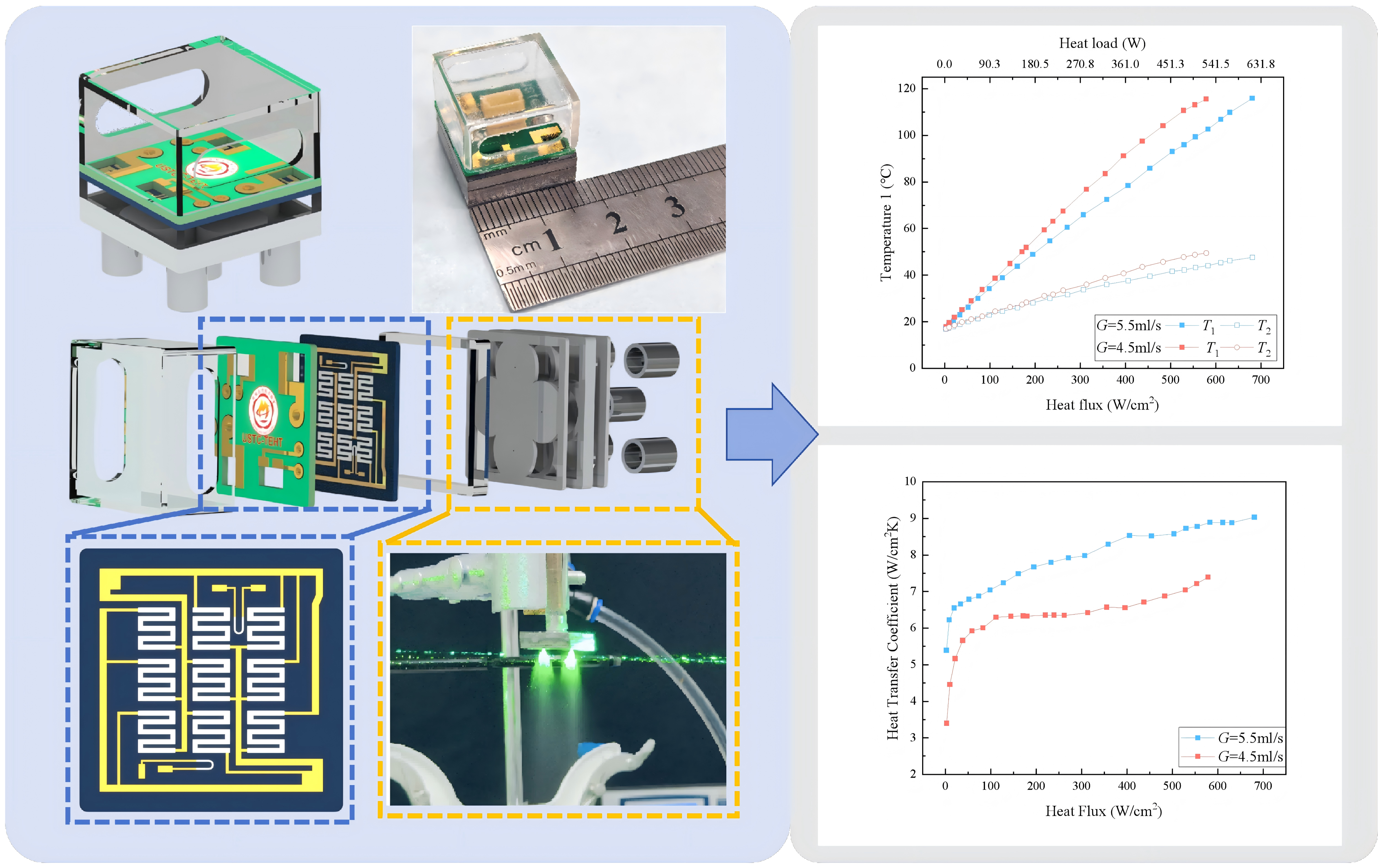
The design of the ultra-thin spray array was optimized based on the prior findings of our research group. Figure 1 illustrates the spray characteristics of the low-pressure pressure-swirl nozzle developed by the research team. This nozzle configuration features a simplified structure and enables fine atomization under low-pressure conditions, providing valuable insights for the design of ultra-thin spray arrays in compact spaces. The ultra-thin spray array described herein consists of a cover plate, swirl chamber, and nozzle orifices, with all components fabricated from 316L stainless steel foils. As shown in Figure 2a, these components were brazed and integrated under vacuum conditions, resulting in an ultra-thin spray array with dimensions of 17 × 17 × 3.5 mm. As shown in Figure 2b, the atomization characteristics of the ultra-thin spray were measured under the laser irradiation of the phase Doppler particle analyzer (PDPA). Given the short nozzle-to-chip distance of only 2 mm, the physical characteristics of the spray were measured at this specific spacing, as illustrated in Figure 2c. Selecting a typical operating condition, when the flow rate (G) reached 4.5 mL/s, the pressure difference (ΔP) between the nozzle inlet and outlet reached 0.3 MPa. The X-axis was defined along a direction in the horizontal plane passing through the spray center, and spray characteristics were measured at 1 mm intervals along this axis. The velocity component in the primary spray direction was defined as vz, and the velocity component along the X-axis was defined as vx. The maximum velocity in the primary spray direction (vz) was measured at 16.8 m/s, while the maximum X-axis velocity (vx) reached 5.3 m/s. Simultaneously, the Sauter mean diameter (d32) of the spray was found to be up to 29.8 μm. According to the research of Banerjee et al.[32], the Sauter mean diameter (d32) has been proven to be a suitable droplet size, indicating excellent near-field atomization performance of the ultra-thin spray.

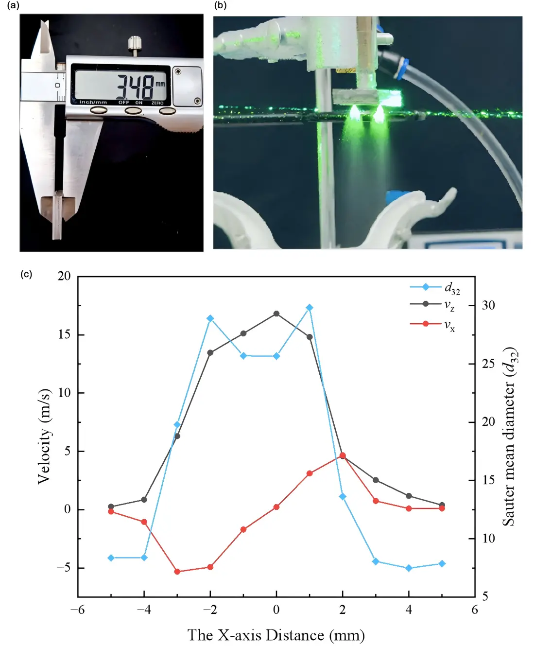
Figure 2. The micro ultra-thin spray array. (a) Hickness measurement; (b) PDPA instrument measures spray characteristics; (c) Spray characteristics of ultra-thin nozzles. PDPA: phase Doppler particle analyzer.
2.2 Thermal test chip
To better align with practical application scenarios, a thermal test chip was fabricated on a 6-inch single-crystal silicon wafer substrate, integrating nine parallel serpentine analog heating circuits and two platinum temperature sensors (4-wire RTDs). As shown in Figure 3, the core fabrication processes include silicon dioxide insulating layer deposition, patterned platinum deposition, patterned gold deposition, and PCB wire bonding. To enable power supply and temperature sensing for the thermal test chip, it was bonded to a custom-designed PCB substrate. As shown in Figure 4, the PCB substrate was sized at 17 × 17 mm (matching the thermal test chip dimensions), with windows etched at positions corresponding to the gold-plated wire bonding pads on the chip. Gold was deposited around the PCB window openings, followed by wire bonding to electrically connect the chip leads to the gold-plated pads on the PCB. Terminal sockets were mounted on the PCB, where the gold-plated regions were interconnected to the socket pins via internal traces. Power supply to the chip and signal transmission from the sensors were realized by plugging in compatible terminal cables. As shown in Figure 5, integration of the thermal test chip with the aforementioned ultra-thin nozzle array yielded a compact spray cooling device.

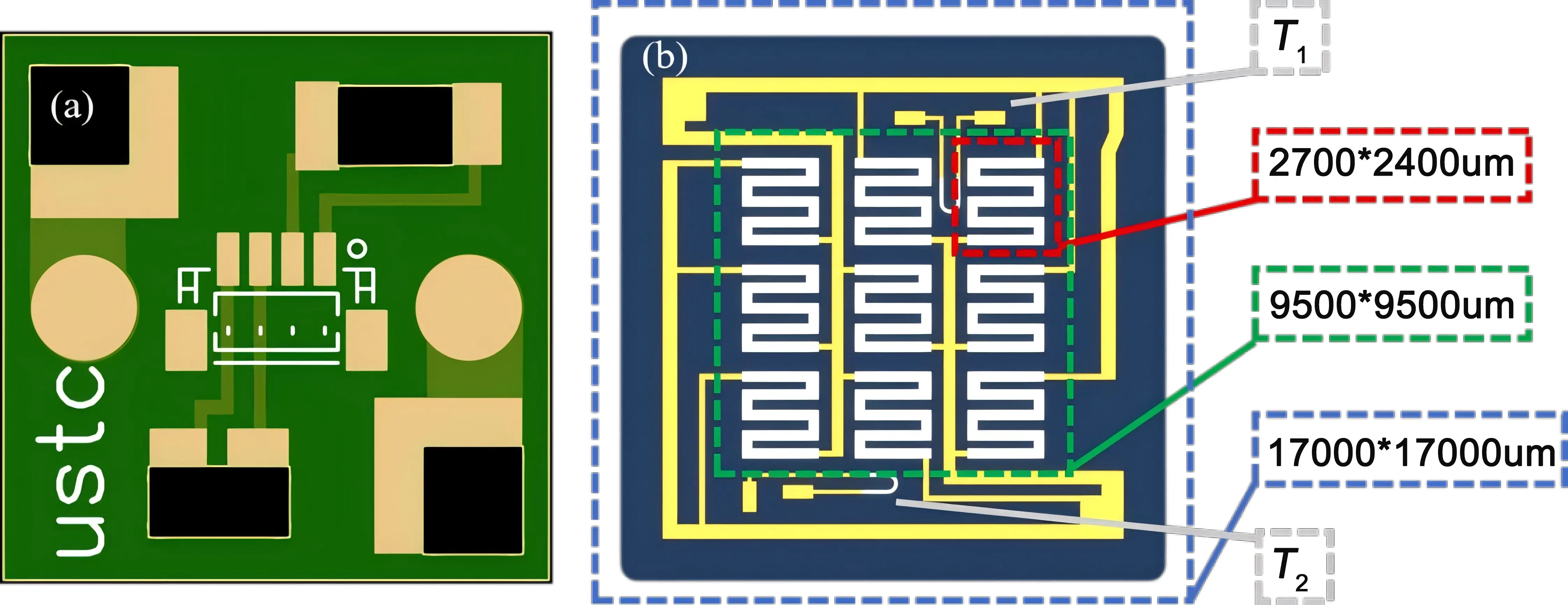
Figure 4. The silicon-based thermal test chip and Its corresponding PCB substrate (showing the position of the platinum resistance temperature sensors T1 and T2). PCB: printed circuit board.
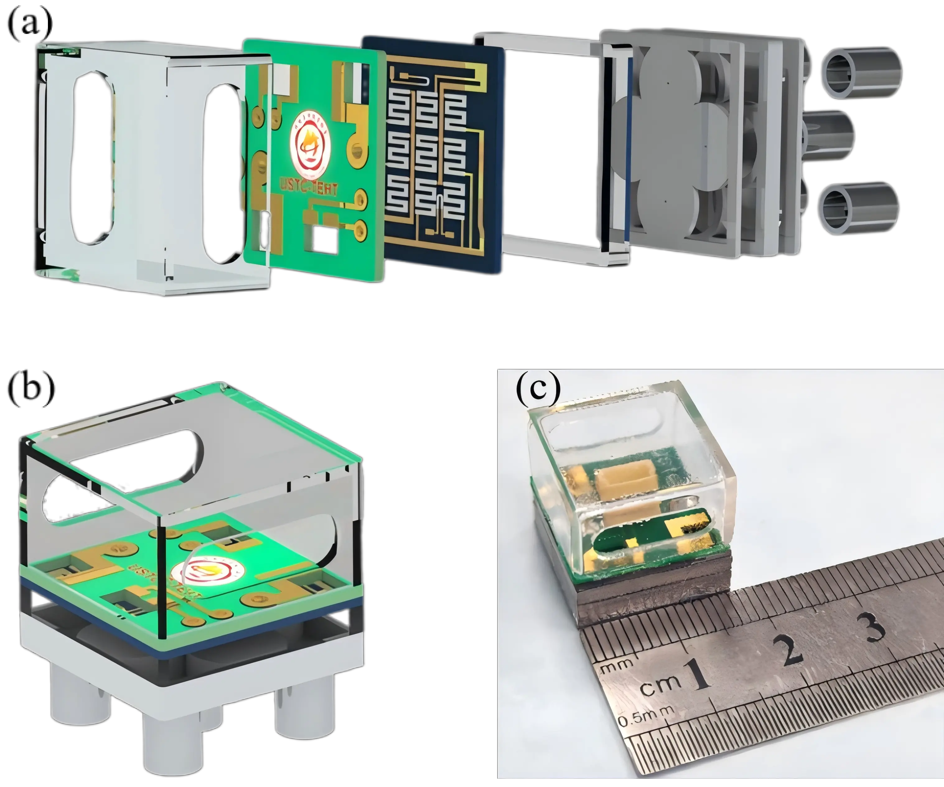
Figure 5. The thermal test chip (a) the exploded view; (b) Overll view; (c) Dimensional measurement.
2.3 Experimental apparatus and procedure
To investigate the heat transfer performance of the ultrathin spray array on silicon-based thermal test chips, a closed-loop test system was constructed in this study. The schematic diagram of the system is presented in Figure 6.
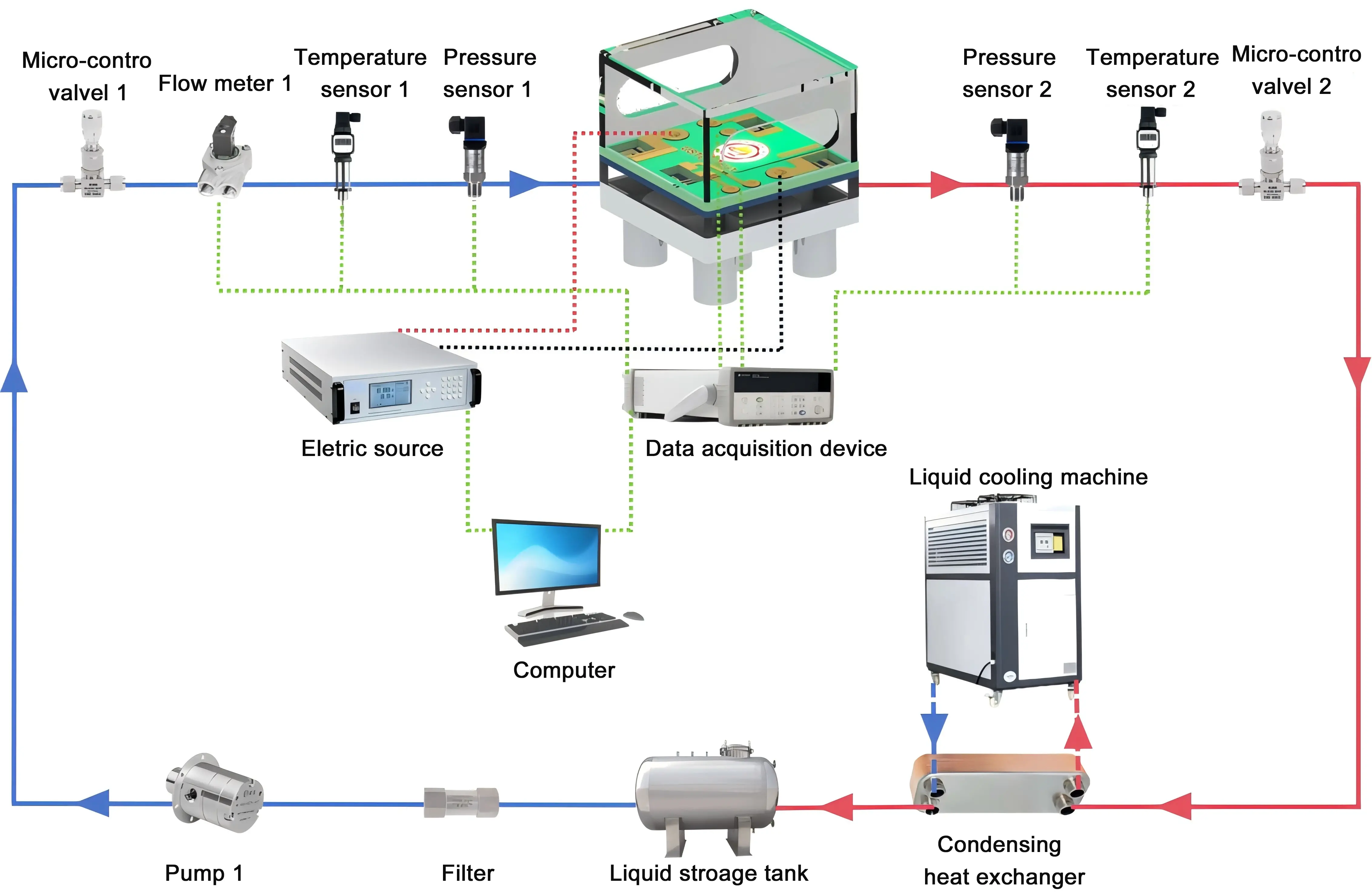
The heating system comprises a silicon-based thermal test chip and a programmable DC power supply. The power supply is connected to the thermal test chip via terminal blocks, where specific voltage and current parameters are configured to drive the platinum heater and generate heat.
In the piping system, the cooling working fluid flows from the reservoir through a 20-μm filter, then is pressurized by Pump 1 (Sofu NP-170). After its flow rate is regulated by Micro-regulating Valve 1, the fluid enters the ultra-thin spray array to cool the thermal test chip. Following heat exchange, the working fluid passes through Micro-regulating Valve 2 (for outlet pressure adjustment), and then flows to a plate heat exchanger for cooling before returning to the reservoir.
The liquid cooling system is primarily composed of a 2-kW liquid cooling unit, with ethylene glycol solution as the coolant. Serving as a precooler, the liquid cooling unit is dedicated to regulating the inlet temperature of the working fluid, with a set temperature range of -40 °C to room temperature and a flow rate of 4.0 L/min. It is connected to a plate heat exchanger with a heat transfer area of 0.42 m2.
The data acquisition system comprises a micro flowmeter (Yikong Technology GICAR-1111), a pressure transmitter (Jixun Automation, 0-1.6 MPa), a temperature sensor (Hirschmann PT100), a platinum temperature sensor integrated on the SiC thermal test chip, and a data acquisition unit (Agilent 34790A).
The specific experimental procedures in this study are as follows:
(1) System tightness inspection: Open all valves in the system, connect a helium mass spectrometer leak detector for evacuation, and inject helium at each pipeline component using the helium spray method. The system is deemed tightly sealed if the leak rate is less than 1 × 10⁻⁸ Pa·m3/s.
(2) A specified mass of degassed deionized water is charged into the system. Subsequently, Gear Pump 1 is activated to initiate circulation of the working fluid, and Micro-regulating Valves 1 and 2 are adjusted to maintain a stable flow rate.
(3) The data acquisition system is activated, followed by the liquid cooling heat exchange system and the heating system. The temperature, flow rate, and pressure at the inlet of the thermal test chip are regulated to the preset conditions. Data recording is initiated only after all parameters have remained a steady state for 3 minutes.
2.4 Experimental data processing and uncertainty analysis
To verify whether the electrical heating power of the thermal test chip equals the heat absorbed by the cooling working fluid, the flow rate and inlet/outlet temperatures of the working fluid were measured in single-phase experiments. After thermal balance calculation, the discrepancy between the heat absorbed by the working fluid and the heat generated by the chip was found to be less than 2%, indicating that the insulating foam wrapped around the thermal test chip effectively suppresses convective heat transfer with the ambient air and radiative heat transfer from the surface.
Prior to conducting flow and heat transfer experiments on the thermal test chip, pre-calibration of the two platinum resistance temperature sensors integrated on the chip was required to establish the temperature-resistance relationship. The specific calibration procedure is as follows: The platinum temperature sensors on the thermal test chip are connected to the data acquisition unit via a four-wire configuration, then placed in a temperature-humidity test chamber. The chamber temperature is adjustable and monitored using a thermocouple. After collating the thermocouple-measured temperatures and sensor resistance values, a linear regression analysis is performed to derive the temperature-resistance linear relationship for each sensor.
The heat flux density q of the chip is defined as:
where Q denotes the thermal load of the chip, and A represents the heat-generating area of the chip.
The average surface temperature Tsurf of the chip is defined as:
where T1 and T2 denote the temperatures calculated by the two platinum resistance sensors on the chip. However, considering their layout positions, T1 is more accurate for representing the chip temperature, while T2 serves only as a reference for the chip edge temperature (Figure 4). Δxi represents the thickness of each layer of material film from the platinum resistance circuit layer to the upper surface of the chip, which includes the chromium seed layer between gold and platinum, the gold film, the chromium seed layer between gold and silicon, the silicon dioxide film, and the single-crystal silicon substrate. λi are the thermal conductivities of the corresponding films. For the vertical stacking sequence and spatial distribution of the constituent layers, please refer to Figure 3.
The heat transfer coefficient h on the chip surface during the experiment is defined as:
where Tin denotes the inlet temperature of the spray cooling medium.
During the experiment, the effective thermal resistance R is defined as:
The measurement uncertainty depends on the measurement uncertainties of parameters including thermal power, temperature, flow rate, and pressure. Table 1 lists the measuring instruments involved in the experiment and their accuracies.
Table 1. Measuring instruments and their accuracy./
| Measurement data | Measuring instruments | Range | Precision |
| Chip temperature | Platinum resistance temperature sensor | / | ±1 K |
| Heat load | Eletric source | 0-2 kW | ±1% |
| Inlet temperature | PT100 platinumresistance | -50~150 °C | ±0.15 K |
| Outlet temperature | PT100 platinumresistance | -50~150 °C | ±0.15 K |
| Inlet pressure | Pressure sensors | 0-1,600 KPa | ±3.2 KPa |
| Outlet pressure | Pressure sensors | 0-1,600 KPa | ±3.2 KPa |
| Inlet flow rate | Miniature flowmeter | 1.5-42 L/h | ±0.6 L/h |
According to the law of error propagation, the indirect uncertainty can be described as:
Thus, the indirect relative uncertainty associated with the heat flux density, average surface temperature, surface heat transfer coefficient, and thermal resistance of the thermal test chip are ±0.4%, ±2.7%, ±7.2%, and ±5.3%, respectively.
3. Results and Discussion
To investigate the heat transfer performance under varying flow conditions, spray pressure differences of 0.4 MPa and 0.7 MPa, corresponding to volumetric flow rates of 4.5 mL/s and 5.5 mL/s, respectively, were established by regulating the rotational speed of the gear pump and the opening degree of the micro-adjustment valve. Simultaneously, a constant temperature bath was employed to maintain the inlet fluid temperature at a stable 17 °C. As illustrated in Figure 7a, under both flow regimes, the temperatures measured at the two monitoring points exhibit a linear-like increase with the rise in heat flux. It is observed that the temperature at the central measurement point (T₁) on the heating surface rises relatively rapidly, whereas that at the edge measurement point (T₂) increases rather slowly. Under a volumetric flow rate of 5.5 mL/s, when the heat load was applied to 614.3 W (corresponding to a heat flux density of 680.6 W/cm2), the temperature at measurement point T1 reached 115.8 °C, while the temperature at measurement point T2 was only 47.6 °C, resulting in a temperature difference of 68.2 °C. Owing to the low heat transfer resistance associated with spray cooling, it is inferred that the applied heat flux is primarily transferred via the shortest heat transfer path, i.e., the vertical direction. This localized heat transfer behavior can be explained from the perspective of spray impingement hydrodynamics: the stagnation zone directly beneath the nozzle experiences the highest droplet momentum and the thinnest boundary layer, resulting in the strongest local heat extraction capability. In contrast, the peripheral regions rely on the lateral spreading of the liquid film, where the thermal boundary layer develops gradually and droplet velocity decreases, leading to a reduction in heat transfer efficiency[19]. This mechanism accounts for the significant temperature gradient observed between the central (T1) and edge (T2) measurement points on the chip.
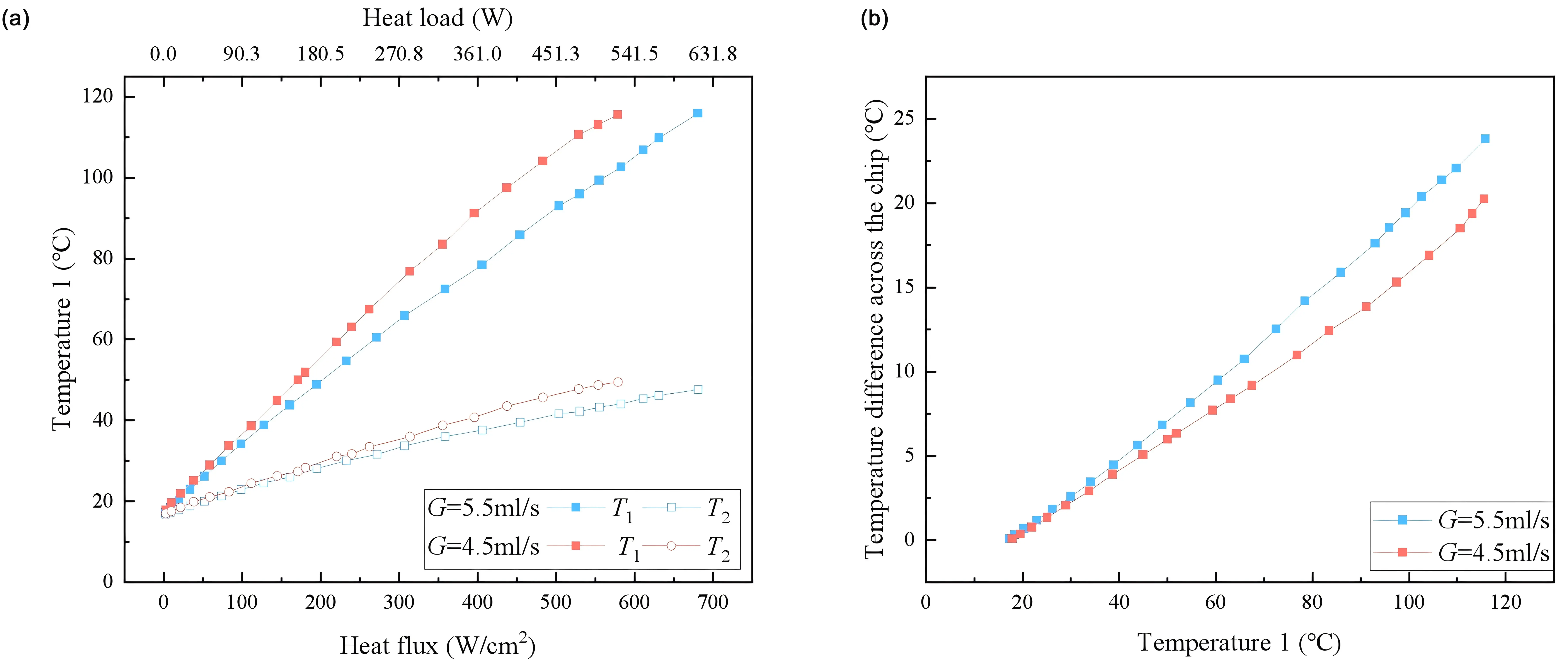
Figure 7. Temperature characteristic curve of spray cooling for the thermal test chip.
As depicted in Figure 7b, under this heat flux condition, the temperature difference between the heating surface of the silicon wafer and the heat exchange surface reaches nearly 24 °C, with the surface temperature of the heat exchange surface being approximately 92 °C at this point. For the thermal test chip fabricated on a single-crystal silicon substrate, the relatively low thermal conductivity of silicon leads to a substantial temperature discrepancy between the heated surface and the heat exchange interface under high heat flux conditions. In addition to further thinning the chip, alternative strategies, such as utilizing advanced semiconductor substrate materials (e.g., silicon carbide), can be employed to mitigate the temperature difference across the two surfaces. Notably, at a volumetric flow rate of 4.5 mL/s, the heat transfer curve exhibits a “steepening” trend starting from a heat load of 500 W. As analyzed in Figure 7b, the surface temperature exceeds 92 °C at this stage, indicating the onset of mild two-phase heat transfer. This phenomenon arises from the presence of a recirculation zone in the spray cooling system[33,34], where localized negative pressure induces “premature boiling”. From the perspective of phase-change heat transfer, this phenomenon can be attributed to the inception of nucleate boiling under subcooled conditions. Local pressure fluctuations induced by the recirculation zone temporarily depress the saturation temperature of the working fluid, thereby reducing the activation energy required for bubble nucleation. Furthermore, the liquid film accumulated in the low-velocity region provides favorable sites for bubble formation and growth, enabling the initiation of two-phase heat exchange even before the average surface temperature reaches the saturation point under ambient pressure. The heat transfer performance discrepancy between the two flow conditions is negligible under low heat flux but becomes increasingly pronounced with rising heat flux. Specifically, at a heat flux density of 520 W/cm2, the temperature at measurement point T₁ in the 5.5 mL/s experimental group is approximately 7 °C lower than that in the 4.5 mL/s group.
Further analysis of heat transfer characteristics was conducted using Figure 8, where subfigures (a) and (b) depict the relationships between heat flux density and heat transfer coefficient, as well as thermal resistance, respectively. As shown in Figure 8a, the heat transfer coefficient curve exhibits an initial rapid increase with rising heat flux density; beyond a heat flux of 50 W/cm2, the growth rate slows down. Notably, the heat transfer coefficient curve for the 4.5 mL/s experimental group lies consistently below that of the 5.5 mL/s group, indicating a significant dependence of the heat transfer coefficient on flow rate. At a heat flux density of 680.6 W/cm2, the heat transfer coefficient of the 5.5 mL/s group reaches 9.03 W/cm2·K, highlighting the excellent heat transfer performance of spray cooling. From the perspective of thermal resistance (the reciprocal of the heat transfer coefficient), the minimum thermal resistance achieved is 0.11 cm2·K/W, which is far superior to the heat transfer performance of manifold microchannels[31].
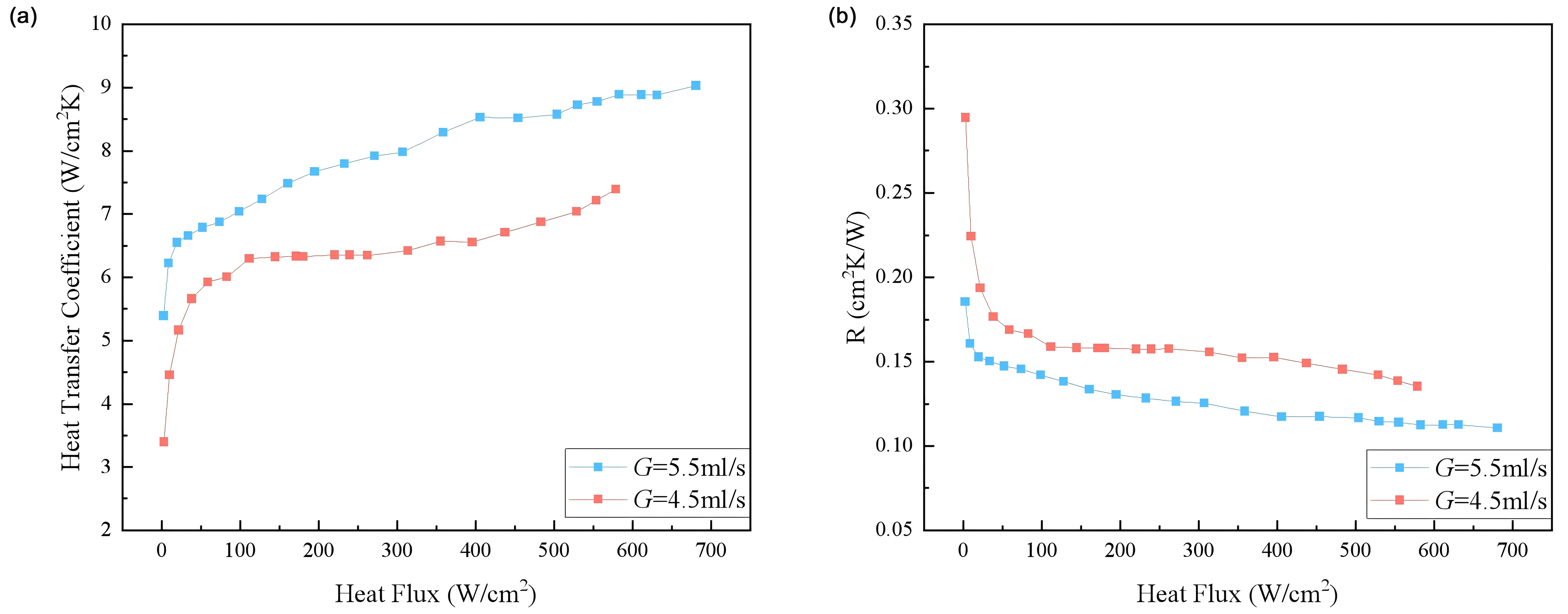
Figure 8. Heat transfer characteristics of spray cooling for the thermal test chip.
4. Conclusions
In conclusion, this study designed, fabricated, and characterized a compact thermal management device integrating an ultra-thin spray array with a silicon-based thermal test chip. For the first time, a precise near-field spray effect was achieved within a compact footprint of 17 mm × 17 mm, enabling the application of spray cooling technology to the thermal management system of silicon-based thermal test chips. This device successfully dissipated a maximum thermal load of 614.3 W. The key conclusions are summarized as follows:
(1) At a volumetric flow rate of 5.5 mL/s, the system successfully withstood an ultra-high heat flux of 680.6 W/cm2 with an ultra-low thermal resistance of 0.11 cm2·K/W, maintaining the central temperature of the chip at 115.8 °C. The corresponding heat transfer coefficient reached 9.03 W/cm2·K, which validates the significant potential of the ultra-thin spray array for achieving high-efficiency thermal management within a minimal spatial footprint.
(2) A significant temperature discrepancy exists between the center and edge of the heating zone (reaching a maximum of 68.2 °C), indicating that spray cooling exhibits strong localized heat transfer behavior. Under high heat flux conditions, an approximate 24 °C temperature difference is observed between the heat-generating surface and the heat-exchange interface of the chip, which is primarily constrained by the thermal conductivity of the single-crystal silicon substrate. To optimize the overall thermal management performance, subsequent work will focus on employing substrate materials with higher thermal conductivity or thinner chip architectures.
(3) Flow Rate Dependence and the “Premature Boiling” Phenomenon: A higher volumetric flow rate (5.5 vs. 4.5 mL/s) yields superior cooling performance across the entire heat flux range, with the advantage becoming more pronounced under conditions of large temperature differences. A steepened heat transfer curve was observed under low flow rate and high heat flux conditions, which signifies the transition from the single-phase to the two-phase heat transfer regime. The localized pressure reduction temporarily alters the local saturation conditions, thereby triggering nucleate boiling.
Acknowledgements
This work was partially carried out at the USTC Center for Micro and Nanoscale Research and Fabrication. We would like to thank Dr. Yi Jin, Dr. Anfeng Shi and Dr. Jie Tian at Experimental Center of Engineering and Material Sciences, USTC for their assistance.
Authors contribution
Zhou R: Conceptualization, data curation, writing-original draft, writing-review & editing.
Cheng W: Funding acquisition, resources, supervision.
Shen Y, Yan J, Chen H: Formal analysis, investigation.
Conflicts of interest
The authors declare no potential conflict of interest exists.
Ethical approval
Not applicable.
Consent to participate
Not applicable.
Consent for publication
Not applicable.
Availability of data and materials
The data and materials could be obtained from the corresponding author upon reasonable request.
Funding
The authors thank the National Natural Science Foundation of China (Grant No. 52376153), the Major Science and Technology Special Project of Anhui Province (Grant No. 202203a07020023), the Young Eagle Fund of the University of Science and Technology of China (Grant No. CY2025G008B), the Students ' Innovation and Entrepreneurship Foundation of USTC (Grant No.CY2025G008B), and the Innovation Special Project for the Integration of Science and Education (Grant No. SITPKJRH-2025-10).
Copyright
© The Author(s) 2026.
References
-
1. Ren H, Chen Z, Liu JH, Yang CT, Yang B, Vaisband B, et al. Integrated passive devices in the silicon-interconnect fabric. In: 2025 IEEE 75th Electronic Components and Technology Conference (ECTC); 2025 May 27-30; Dallas, USA. Piscataway: IEEE; 2025. p. 1994-1998.[DOI]
-
2. Jiao B, Xu L, Yu X, Yang H, Zhu H, Wang Y, et al. FPIA: Communication-aware multi-chiplet integration with field-programmable interconnect fabric on reusable silicon interposer. IEEE Trans Circuits Syst I. 2024;71(9):4156-4168.[DOI]
-
3. Bender E, Bernstein JB, Boning DS. Modern trends in microelectronics packaging reliability testing. Micromachines. 2024;15(3):398.[DOI]
-
4. Nisa UU, Bashir J. Towards efficient on-chip communication: A survey on silicon nanophotonics and optical networks-on-chip. J Syst Archit. 2024;152:103171.[DOI]
-
5. Son K, Choi S, Kim K, Yoon J, Lee J, Suh H, et al. High-speed interconnect design of silicon interposer based heterogeneous integration for ai computing. In: 2024 IEEE 33rd Conference on Electrical Performance of Electronic Packaging and Systems (EPEPS); 2024 Oct 6-9; Toronto, Canada. Piscataway: IEEE; 2024. p. 1-3.[DOI]
-
6. Kundu Y, Kaur M, Wig T, Kumar K, Kumari P, Puri V, et al. A comparison of the cerebras wafer-scale integration technology with nvidia gpu-based systems for artificial intelligence. arXiv:2503.11698 [Preprint]. 2025.[DOI]
-
7. Talpes E, Williams D, Das Sarma D. DOJO: The microarchitecture of tesla’s exa-scale computer. In: 2022 IEEE hot chips 34 symposium (HCS). IEEE; 2022. p. 1-28.[DOI]
-
8. Woon WY, Kasperovich A, Wen JR, Hu KK, Malakoutian M, Jhang JH, et al. Thermal management materials for 3D-stacked integrated circuits. Nat Rev Electr Eng. 2025;2(9):598-613.[DOI]
-
9. Riccio M, Castellazzi A, De Falco G, Irace A. Experimental analysis of electro-thermal instability in SiC Power MOSFETs. Microelectron Reliab. 2013;53(9-11):1739-1744.[DOI]
-
10. Sui J, Yao T, Zou J, Liao S, Zhang HF. A switchable dual-mode integrated photonic multilayer film with highly efficient wide-angle radiative cooling and thermal insulation for year-round thermal management. Int J Heat Mass Transf. 2025;241:126783.[DOI]
-
11. Chase NS. Physics based reliability analysis of the silicon interconnect fabric. Los Angeles: University of California; 2021. Available from: https://escholarship.org/content/qt34f1m6wn/qt34f1m6wn_noSplash_2ff4e196c9e95a5c80d3a2f67d20276c.pdf
-
12. Shah U, Mogera U, Ambhore P, Vaisband B, Iyer SS, Fisher TS. Dynamic thermal management of silicon interconnect fabric using flash cooling. In: 2019 18th IEEE Intersociety Conference on Thermal and Thermomechanical Phenomena in Electronic Systems (ITherm); 2019 May 28-31; Las Vegas, USA. Piscataway: IEEE; 2019. p. 1228-1233.[DOI]
-
13. Chen X, Hu C, Liang J, Li J, Lu L, Wu Y, et al. Efficient two-phase liquid cooling and optimization technology on the chip side based on high-power data centers: Summary and prospects. Renew Sustain Energy Rev. 2025;223:115994.[DOI]
-
14. Chen H, Zhang T, Gao Q, Lv J, Chen H, Huang H. Thermal management enhancement of electronic chips based on novel technologies. Energy. 2025;316:134575.[DOI]
-
15. Yang S, Cao B, Wu Z, Hong S, Xu H, Sheng K. Experimental study of a SiC manifold microchannel heat sink under background and hotspot heating scenarios at ultra-high heat flux. Int J Heat Mass Transf. 2026;254:127657.[DOI]
-
16. Hu Y, Lei Y, Liu X, Yang R. Record-high heat transfer performance of spray cooling on 3D-printed hierarchical micro/nano-structured surface. Sci Bull. 2025;70(2):223-231.[DOI]
-
17. Chen H, Ruan XH, Peng YH, Wang YL, Yu CK. Application status and prospect of spray cooling in electronics and energy conversion industries. Sustain Energy Technol Assess. 2022;52:102181.[DOI]
-
18. Benther JD, Pelaez-Restrepo JD, Stanley C, Rosengarten G. Heat transfer during multiple droplet impingement and spray cooling: Review and prospects for enhanced surfaces. Int J Heat Mass Transf. 2021;178:121587.[DOI]
-
19. Liang G, Mudawar I. Review of spray cooling–Part 1: Single-phase and nucleate boiling regimes, and critical heat flux. Int J Heat Mass Transf. 2017;115:1174-1205.[DOI]
-
20. Liang G, Mudawar I. Review of spray cooling–Part 2: High temperature boiling regimes and quenching applications. Int J Heat Mass Transf. 2017;115:1206-1222.[DOI]
-
21. Opoku R, Kizito JP. Experimental investigation of heat transfer characteristics and performance of smooth and wicking surfaces in spray cooling for high heat flux applications. Results Eng. 2020;6:100119.[DOI]
-
22. Zhou R, Pan YH, Zheng L, Fu H, Shen Y, Hao M, et al. Study on heat transfer enhancement of spray cooling with bionic vein channel structured surface. Appl Therm Eng. 2024;246:122977.[DOI]
-
23. Zhou R, Chen H, Cheng WL. Experimental study on enhancement of heat transfer by spray cooling of leaf vein surface with surfactant. In: Proceeding of THMT-25 turbulence, heat and mass transfer 11, 21-25 July 2025,Tokyo, Japan. Begellhouse; 2025. p. 6.[DOI]
-
24. Jiang LJ, Jiang SL, Cheng WL, Nian YL, Zhao R. Experimental study on heat transfer performance of a novel compact spray cooling module. Appl Therm Eng. 2019;154:150-156.[DOI]
-
25. Carneiro MVP, Provensi A, Ferreira JCA, Cavicchioli P, Pereira M, Barbosa JR Jr. Experimental analysis of a compact cooling system containing an enhanced-surface spray heat sink. Exp Therm Fluid Sci. 2024;151:111078.[DOI]
-
26. Zhou R, Fu H, Yan J, Shen Y, Chen H, Cheng WL. Experimental investigation on heat transfer characteristics of arrayed spray cooling plate at various inclination. Int Commun Heat Mass Transf. 2025;162:108666.[DOI]
-
27. Fu H, Chen H, Zheng L, Zhao R, Han L, Liu J, et al. Experimental study on two-phase heat transfer performance of integrated compact spray cold plate. Appl Therm Eng. 2024;255:123948.[DOI]
-
28. Siddiqui OK, Zubair SM. Efficient energy utilization through proper design of microchannel heat exchanger manifolds: A comprehensive review. Renew Sustain Energy Rev. 2017;74:969-1002.[DOI]
-
29. Pan Y, Chen H, Shen Y, Cheng W. Experimental study on the flow and heat transfer characteristics of pin-fin manifold microchannel heat sink. J Phys: Conf Ser. 2024;2683(1):012031.[DOI]
-
30. van Erp R, Soleimanzadeh R, Nela L, Kampitsis G, Matioli E. Co-designing electronics with microfluidics for more sustainable cooling. Nature. 2020;585(7824):211-216.[DOI]
-
31. Shen YT, Dai YB, Lu JX, Zhou R, Chen H, Cheng WL. Experiment on enhanced heat transfer of embedded manifold Tesla-patterned microchannel heat sink. Int Commun Heat Mass Transf. 2025;165:109050.[DOI]
-
32. Banerjee N, Tropea C, Seshadri S. Methodology to compute spray cooling in the nucleate boiling regime. Int J Heat Mass Transf. 2024;225:125375.[DOI]
-
33. Kim J. Spray cooling heat transfer: The state of the art. Int J Heat Fluid Flow. 2007;28(4):753-767.[DOI]
-
34. Ding JW, Li GX, Yu YS, Li HM. Numerical investigation on primary atomization mechanism of hollow cone swirling sprays. Int J Rotating Mach. 2016;2016:1201497.[DOI]
Copyright
© The Author(s) 2026. This is an Open Access article licensed under a Creative Commons Attribution 4.0 International License (https://creativecommons.org/licenses/by/4.0/), which permits unrestricted use, sharing, adaptation, distribution and reproduction in any medium or format, for any purpose, even commercially, as long as you give appropriate credit to the original author(s) and the source, provide a link to the Creative Commons license, and indicate if changes were made.
Publisher’s Note
Science Exploration remains a neutral stance on jurisdictional claims in published
maps
and institutional affiliations. The views expressed in this article are solely those
of
the author(s) and do not reflect the opinions of the Editors or the publisher.
Share And Cite


Science Exploration Style
Zhou R, Shen Y, Yan J, Chen H, Cheng WL. Ultra-thin spray cooling for high-power-density silicon chips. Thermo-X. 2026;2:202603. https://doi.org/10.70401/tx.2026.0014
Tips
Copy completed.
Submit a Manuscript
Author Instructions
Cite this Article
Article Metrics
0
View
0
Download
Cited
Article Updates

Science Exploration Style
Zhou R, Shen Y, Yan J, Chen H, Cheng WL. Ultra-thin spray cooling for high-power-density silicon chips. Thermo-X. 2026;2:202603. https://doi.org/10.70401/tx.2026.0014
copy
Share Link
copy