Advances in conductive microneedles: From fabrications to applications
Qi Zhang
1
,
Sukrit Gaira
1
,
Junyan Lai
1
,
Rongfeng Wang
1
,
Yuanyi Zhao
1
,
Leo Wu
1

,
Shi-Yang Tang
1,2,*
,
Qingtian Zhang
1,*
*Correspondence to:
Qingtian Zhang, School of Mechanical and Manufacturing Engineering, University of New South Wales, Sydney, NSW 2052, Australia.
E-mail: qingtian.zhang@unsw.edu.au
Shi-Yang Tang, School of Mechanical and Manufacturing Engineering, University of New South Wales, Sydney, NSW 2052, Australia. E-mail: shiyang.tang2@unsw.edu.au
Shi-Yang Tang, School of Mechanical and Manufacturing Engineering, University of New South Wales, Sydney, NSW 2052, Australia. E-mail: shiyang.tang2@unsw.edu.au
Smart Mater Devices. 2026;2:202613. 10.70401/smd.2026.0034
Received: March 30, 2026Accepted: May 29, 2026Published: May 29, 2026
This article belongs to the Special lssue Micro-Nano Probes and Biosensors for Advanced Diagnostics and Therapeutics
Abstract
Conductive microneedles (CMNs) combine the minimally invasive characteristics of microneedles with the electrical functionality required for sensing, recording, stimulation, and controlled drug delivery. By penetrating the stratum corneum with reduced pain and tissue damage, they provide efficient access to the skin microenvironment and have shown strong potential in wearable healthcare, precision diagnostics, and intelligent therapeutics. Despite these advantages, challenges remain in balancing mechanical robustness with electrical functionality, improving fabrication precision and reproducibility, maintaining interfacial stability, and achieving scalable manufacturing. In this review, the major fabrication routes for CMNs are summarized and compared in terms of forming principles, material compatibility, and conductivity-introduction strategies. Secondly, research on the key performances of CMNs is discussed. After that, the applications of CMNs in electrochemical sensing, bioelectrical signal acquisition, electrostimulation therapy, and drug delivery are overviewed, followed by a brief discussion of current challenges and future perspectives.
Keywords
Conductive microneedles, transdermal device, fabrication strategies, electrochemical sensing, bioelectrical recording, drug delivery
1. Introduction
Microneedles are a minimally invasive device made from a variety of materials such as biomaterials, metals, polymers, ceramics, and composites. It provides a gentler and more efficient intermediate path between traditional subcutaneous injections and regular percutaneous administration, which has gained significant attention in recent years[1]. The outermost stratum corneum of the skin is the main barrier for the transdermal transport of drugs and biomolecules, while microneedles can penetrate the stratum corneum at the micron scale to deliver drugs to the epidermis or superficial dermal area while avoiding deep irritation of nerve endings and capillaries, so it usually has the advantages of minimally invasive, low pain, less bleeding, lower risk of infection, and high patient compliance[2].
On the basis of the continuous development of microneedling technology, conductive microneedles (CMNs) have further endowed microneedles with electrical functions, expanding them from a simple mechanical puncture or drug delivery platform to a functional device with signal transmission, interface electrochemical reaction, and in-situ detection capabilities. Compared with ordinary microneedles, the core advantage of CMNs is that they can directly contact the more electrically active microenvironment in the skin after penetrating the stratum corneum, so it is regarded as an important source of bioinformation suitable for minimally invasive health monitoring[3]. In addition, CMNs can also reduce the impedance of the skin-electrode interface, reduce the dependence of traditional wet electrodes on conductive gels, and improve the stability and signal-to-noise ratio (SNR) of bioelectrical signal acquisition[4,5]. Therefore, CMNs have built an integrated platform for a puncture interface, electrical conversion, and real-time output, which is an important bridge connecting the skin microenvironment and electronic systems.
The application value of CMNs is mainly reflected in three aspects. First, in the field of biosensing and disease monitoring, it can use interstitial fluid, which is a biofluid highly related to blood components, to achieve minimally invasive, continuous, and wearable health monitoring, and provide support for personalized medicine and real-time diagnosis[6,7]. Second, in the field of bioelectrical signal acquisition and human-machine interface, CMNs can be used as dry electrodes for bioelectrical signal recording to improve contact stability and signal fidelity in complex skin environments[5]. Third, in the direction of integration of treatment and diagnosis and treatment, conductive microneedling can also be combined with electrical stimulation, drug delivery, and closed-loop feedback systems to build an intelligent microneedling platform integrating detection, response, and treatment[8]. These diverse applications also place stringent requirements on CMN design. A good CMN should combine sufficient mechanical strength for reliable skin penetration, appropriate stiffness and post-insertion compliance for stable tissue interfacing, high electrical conductivity for functional performance, and good biocompatibility for safe use. These features are governed by the combined effects of material composition, needle geometry, dimensions, and array design.
This review article summarizes CMNs, with particular emphasis on their fabrication technologies and application potential (Figure 1). First, the major fabrication strategies are outlined and compared, including powder-based fabrication, photopolymerization-based manufacturing, material extrusion, and mold-based replication, with attention to their forming principles, material compatibility, conductivity-introduction routes, advantages, and limitations. Next, the key evaluation dimensions of CMNs, including mechanical performance, geometric fidelity, electrical functionality, and biocompatibility, are discussed. Representative applications in electrochemical biosensing, bioelectrical signal acquisition, electrostimulation, and electrically controlled drug delivery are then presented, followed by current challenges and future perspectives.
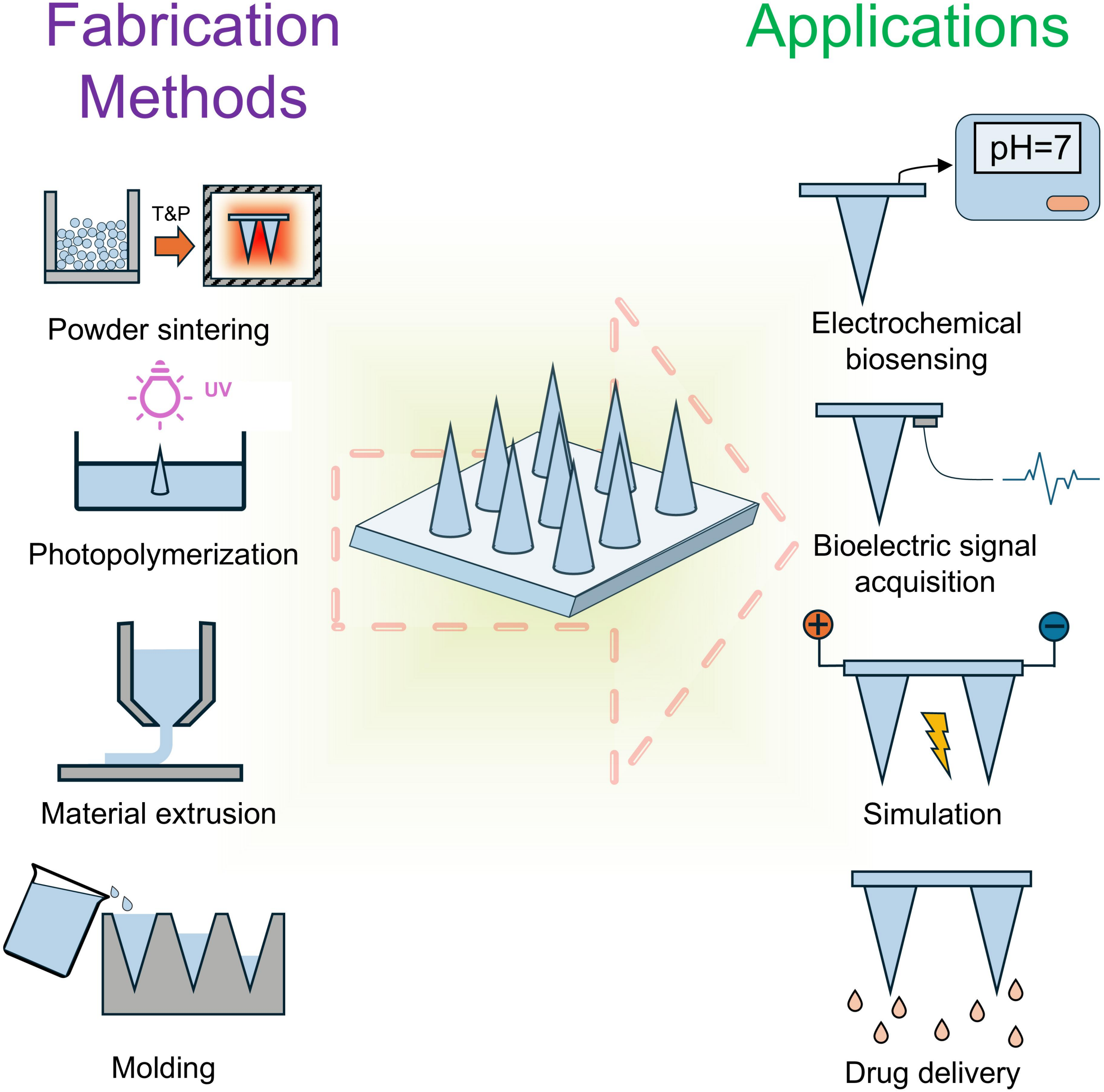
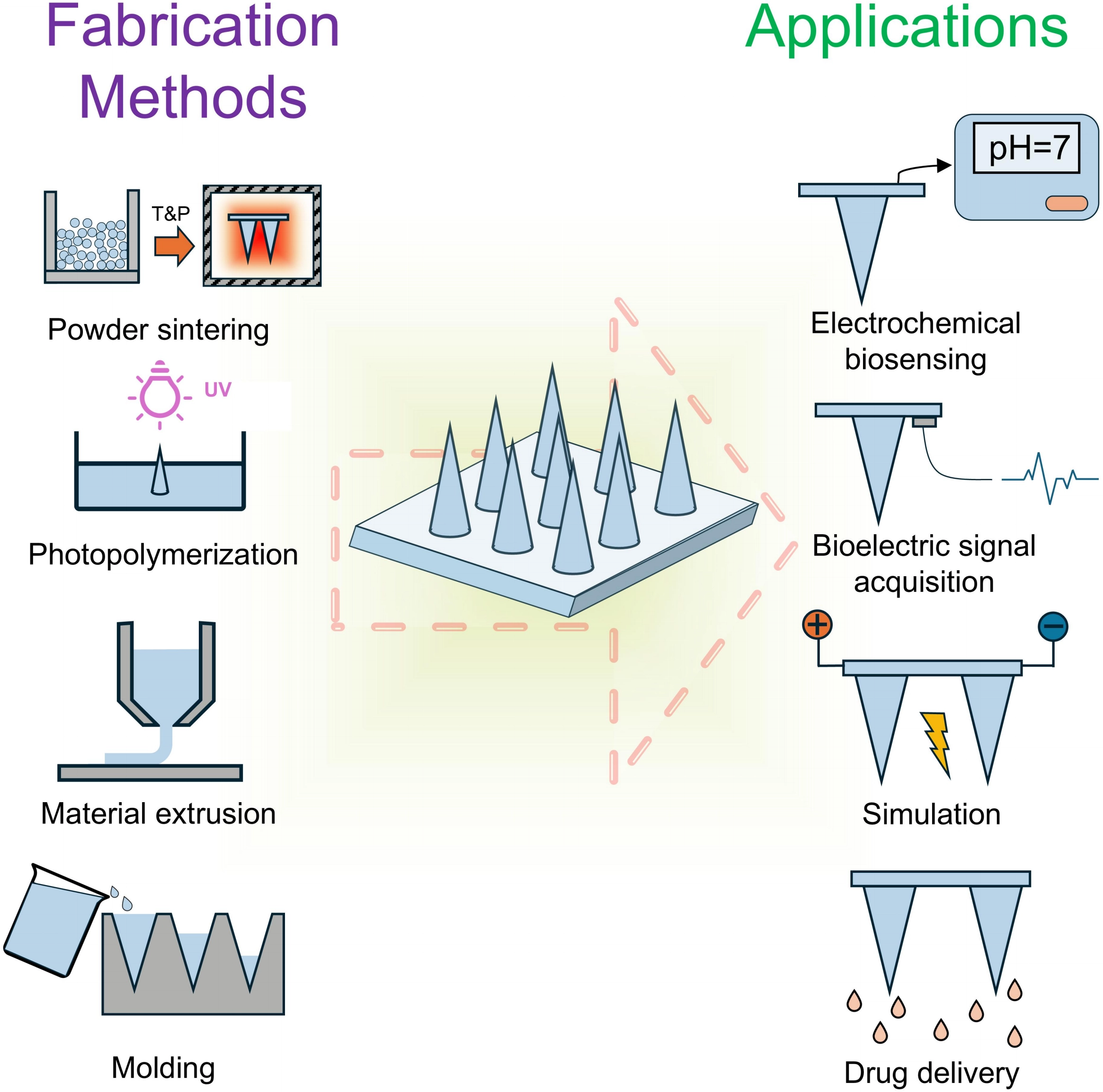
Figure 1. CMNs fabrication technologies and applications. CMNs: conductive microneedles.
The scope of this review is primarily focused on CMNs that possess intrinsic electrical functionality or are specifically designed for electrical sensing, signal acquisition, stimulation, or electrically assisted therapeutic applications. Conventional non-conductive microneedles intended solely for passive drug delivery, such as purely dissolving or biodegradable microneedle systems without conductive components, are not discussed.
2. Materials for Conductive Microneedles
The performance of CMNs is dictated by the properties of their constituent materials. Consequently, the fabrication of CMNs necessitates a strategic balance between reliable electrical conductivity and essential functional requirements, including mechanical integrity, skin penetrability, biocompatibility, and long-term interfacial stability. Given these multifaceted demands, diverse material systems present varying parameters (Table 1).
Table 1. Comparison of representative material categories used in conductive microneedles.
| Material | Electrical conductivity | Mechanical properties (Young’s modulus) | Biocompatibility | References |
| Metals | ~106 - 107 S/m | ~50 - 200 GPa | Generally good, but possible mechanical mismatch or corrosion issues | [9-11] |
| Conductive polymers | ~100 - 105 S/m | ~1 MPa - 1 GPa | Good biointerface compatibility | [12-14] |
| Carbon-based nanocomposites | ~10-1 - 104 S/m | ~1 MPa - 10 GPa | Tunable biocompatibility | [15,16] |
| Conductive hydrogels | ~10-3 - 102 S/cm | ~1 kPa - 10 MPa | Excellent tissue compatibility | [17,18] |
2.1 Metal
Metallic materials are among the earliest and most widely investigated material systems for CMNs because of their excellent electrical conductivity, high mechanical strength, and reliable skin penetration capability[19]. Compared with polymer-based systems, metallic CMNs can better maintain structural integrity during insertion while providing stable electrical pathways for sensing, recording, stimulation, and electrically controlled drug delivery applications.
Among these materials, medical-grade 316L stainless steel has been extensively used due to its favorable combination of mechanical robustness, corrosion resistance, biocompatibility, and manufacturability which provides interconnected pore networks beneficial for drug loading and surface functionalization[20].
Gold (Au) is widely employed in CMNs, particularly for electrochemical biosensing, owing to its high conductivity, corrosion resistance, and excellent biocompatibility. Au is commonly introduced through sputtering or other metallization processes to form conductive layers on polymeric microneedles, while also enabling surface biofunctionalization[21]. Silver and nickel have also been explored for conductive coatings and electrode fabrication due to their favorable electrical and electrochemical properties[22]. In particular, as discussed in detail in the following sections, Choi et al. employed Ti/Cu seed layer deposition followed by Ni electroplating to construct conductive microneedle electrode arrays with enhanced electroactivity and structural stability[23]. Despite their excellent electrical conductivity and mechanical robustness, metallic CMNs still face several challenges, including high stiffness, insertion-associated tissue irritation risks, complex surface functionalization procedures, biofouling susceptibility, and relatively high fabrication cost[24].
2.2 Conductive polymers
Conductive polymers have become an important material class for CMNs due to their flexibility, intrinsic conductivity, and good compatibility with bioelectronic systems. Compared with metallic materials, conductive polymers generally exhibit lower stiffness, making them particularly suitable for wearable sensing and electrophysiological recording applications[25].
A major advantage of conductive polymers is their mixed ionic/electronic conductivity, which facilitates efficient charge transfer at the electrode-tissue interface. This property can help reduce interfacial impedance and improve signal transmission stability, which is important for obtaining stable and low-noise physiological data during long-term bioelectrical recording.
Among various systems, PEDOT:PSS is one of the most widely used conductive polymers because of its high conductivity, biocompatibility, electrochemical stability, and solution processability. It has been employed in conductive coatings, electrode functionalization, and printable conductive inks for CMNs and bioelectronic devices[26]. Polyaniline and polypyrrole have also attracted attention due to their tunable conductivity, electroactivity, and compatibility with biosensing applications[27]. In addition, conductive photocurable resin systems have enabled the direct fabrication of conductive microstructures through photopolymerization-based additive manufacturing technologies[28].
Another important feature of conductive polymers is their strong compatibility with surface functionalization, allowing the integration of biomolecules, enzymes, and electroactive interfaces for sensing and therapeutic applications. However, compared with metallic materials, conductive polymers generally possess lower mechanical strength and may suffer from structural instability under repeated deformation or long-term operation[29]. Therefore, conductive polymers are often combined with conductive fillers, metallic coatings, or composite structures to improve their overall mechanical and electrical performance.
2.3 Carbon-based conductive composites
Carbon-based conductive composites have been widely investigated for CMNs due to their tunable electrical properties, good electrochemical activity, and compatibility with polymer-based fabrication processes. Typical conductive fillers include carbon nanotubes, graphene, and carbon black, which are commonly incorporated into polymer matrices such as polylactic acid (PLA), SU-8, and photocurable resins to construct conductive composite microneedles[30-33].
The electrical conductivity of these composites is primarily achieved through the formation of percolative conductive networks within the insulating matrix[32]. By adjusting filler type and loading concentration, the conductivity and electrochemical performance of CMNs can be effectively tuned. In addition to introducing conductivity, carbon-based fillers can also enhance the mechanical properties of polymer systems, thereby improving structural robustness and insertion reliability.
Moreover, carbon nanomaterials exhibit high surface area and favorable electrochemical activity, making them particularly suitable for biosensing interfaces and electrophysiological applications. However, carbon-based conductive composites still face several challenges. Excessive filler loading may lead to particle aggregation, viscosity increase, and poor processability, which can negatively affect mold filling, printing fidelity, and structural uniformity[34]. In addition, improving electrical conductivity often compromises mechanical flexibility or toughness, resulting in a mechanical–electrical tradeoff.
2.4 Conductive hydrogels
Conductive hydrogels have attracted increasing attention in CMNs due to their excellent tissue compatibility, low elastic modulus, and ability to form stable biointerfaces. Compared with conventional rigid conductive materials, conductive hydrogels exhibit mechanical properties closer to biological tissues, enabling improved conformability and reduced interfacial irritation during long-term operation[35]. In addition, their mixed ionic/electronic transport characteristics are beneficial for signal transmission, interfacial charge exchange, and stable wearable sensing[36]. These features make conductive hydrogels particularly promising for applications such as long-term electrophysiological recording, wearable bioelectronics, and neuromodulation interfaces.
Another important advantage of conductive hydrogels is their ability to function simultaneously as conductive materials and biointerface platforms. Their hydrated network structures can support drug loading, biomolecule immobilization, and tissue-interactive functionalities, making them attractive for integrated sensing and therapeutic systems[37]. Moreover, the soft and stretchable nature of hydrogel-based materials allows them to better accommodate repeated deformation and dynamic skin movement during wearable operation.
However, despite these advantages, conductive hydrogels still face several limitations. Their high water content may lead to dehydration and deterioration of electrical or mechanical properties during long-term use[38]. In addition, many hydrogel systems exhibit relatively poor structural stability and insufficient mechanical stiffness for reliable skin penetration[39]. Therefore, conductive hydrogels are often combined with reinforcing substrates, conductive fillers, or composite architectures to balance penetration capability, electrical performance, and biointerface compatibility.
3. Fabrication Strategies for CMNs
Various fabrication routes have been developed for CMNs, including powder-based processing, photopolymerization-based additive manufacturing, material extrusion, and mold-based replication. Each method differs in forming mechanism, material compatibility, and strategies for introducing conductivity. This section provides a systematic overview and comparison of the major fabrication routes for CMNs. Despite the rapid development of these fabrication strategies, significant differences still remain among them in terms of fabrication resolution, array uniformity, batch-to-batch reproducibility, scalability, and manufacturing throughput[4,40].
3.1 Powder-based fabrication
The initial development of microneedles was mainly based on microelectronics and micromachining systems. A review shows that with the rapid development of the semiconductor manufacturing industry in the 90s of the 20th century, the microfabrication technology suitable for microneedle preparation has gradually matured, thus promoting the early development of medical microneedles, and its materials have gradually expanded from silicon to metal, polymer, ceramic, and glass and other multiple systems[41,42]. It is important to clarify that powder sintering is not the logical starting point for microneedle manufacturing, but rather a key branch that emerged to meet specific mechanical performance and multifunctional integration requirements. In this evolutionary stage, traditional microneedles face a significant trade-off between material properties and functional requirements: while metallic microneedles possess excellent mechanical strength, they are severely constrained by traditional processes in terms of drug loading capacity, expansion of internal functional space, and the freedom to design complex functional structures[41]. At the same time, although polymer microneedles can show good processing and moldability, they still have shortcomings in terms of mechanical strength[43]. In this context, porous microneedles with both mechanical support and functional expansion potential have gradually become the focus of research, and the collaborative optimization between mechanical properties, drug loading capacity, and sensing function is realized through pore structure design.
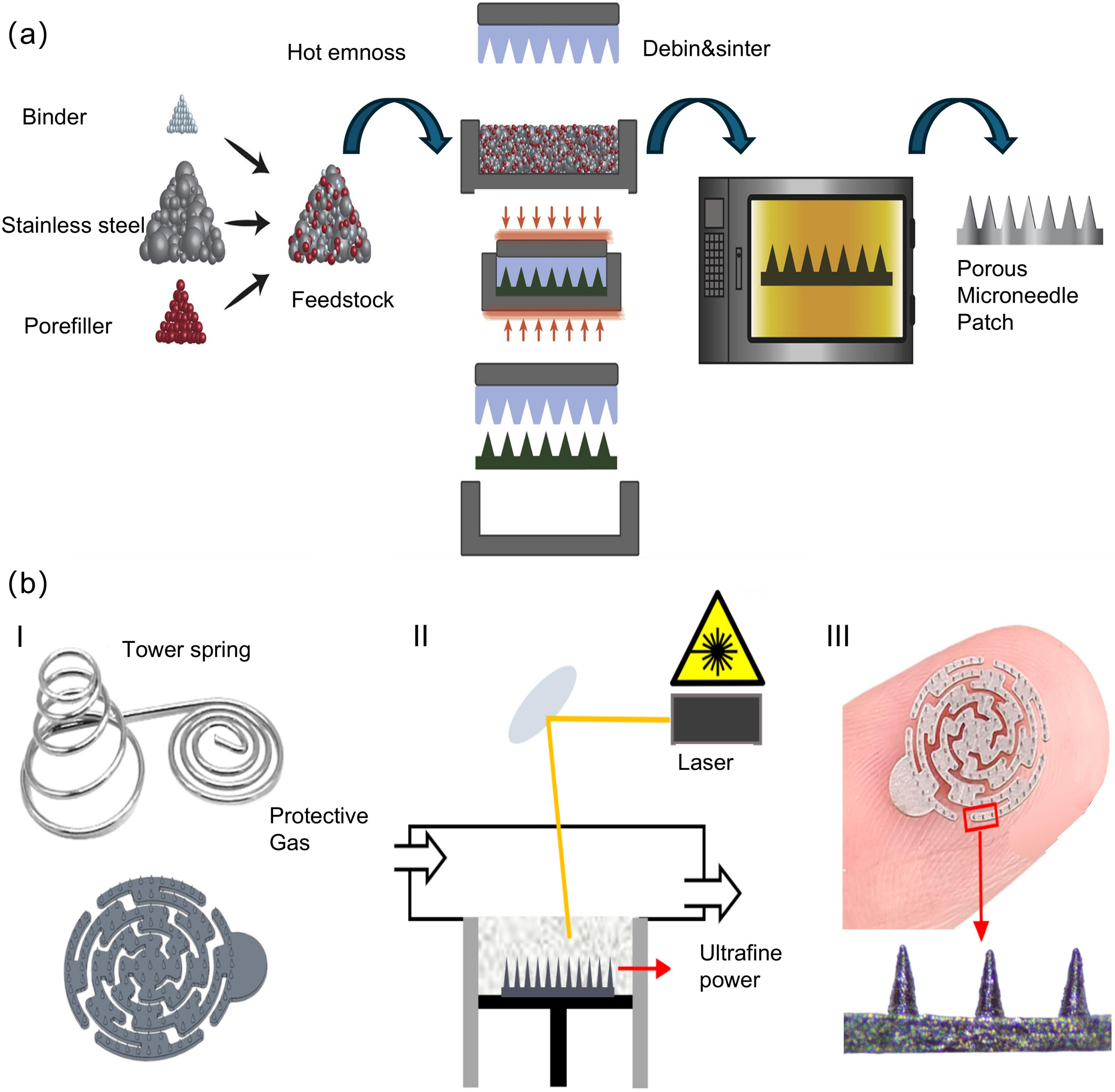
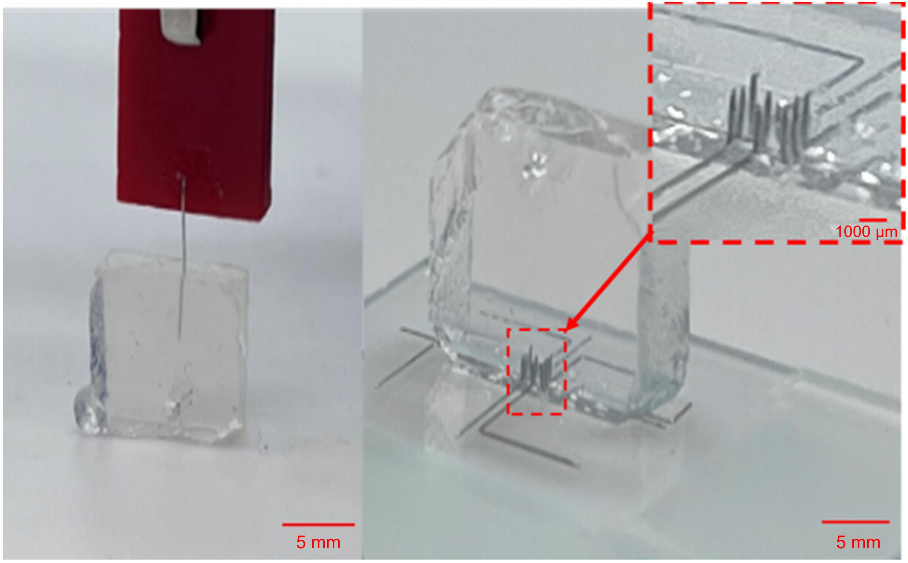
During this stage of development, Cahill et al. reported the use of paraffin adhesives mixed with stainless steel particles and pore fillers as raw materials. The structures were formed via micro hot embossing, followed by moulding with a polydimethylsiloxane (PDMS) mould, sintering at 1,100 °C, and electropolishing to obtain the porous microneedle patches, illustrated in Figure 2. The resulting microneedles exhibited a total porosity of approximately 36%, with an average pore size of 2.22 μm, and 90% of the pores distributed within the range of 1.56-2.93 μm (Figure 3a). Under a load of 19 N, the microneedles were able to effectively penetrate porcine skin and demonstrated significant liquid capillary absorption and transdermal delivery capability[20].
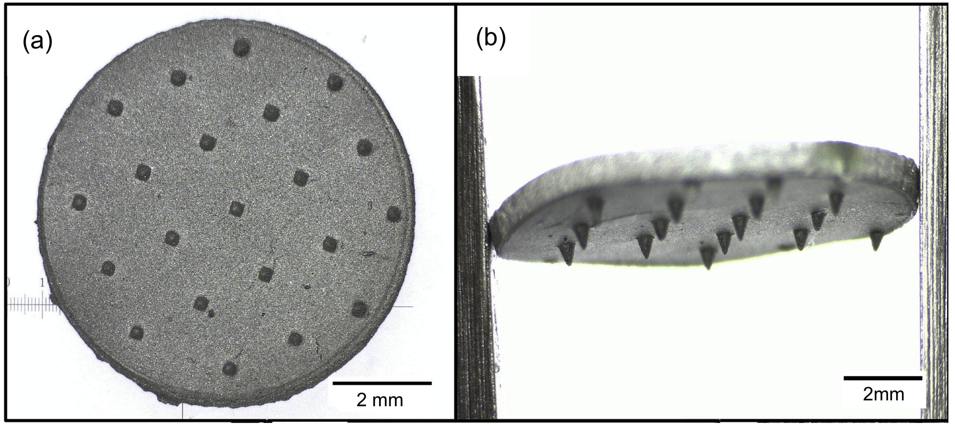
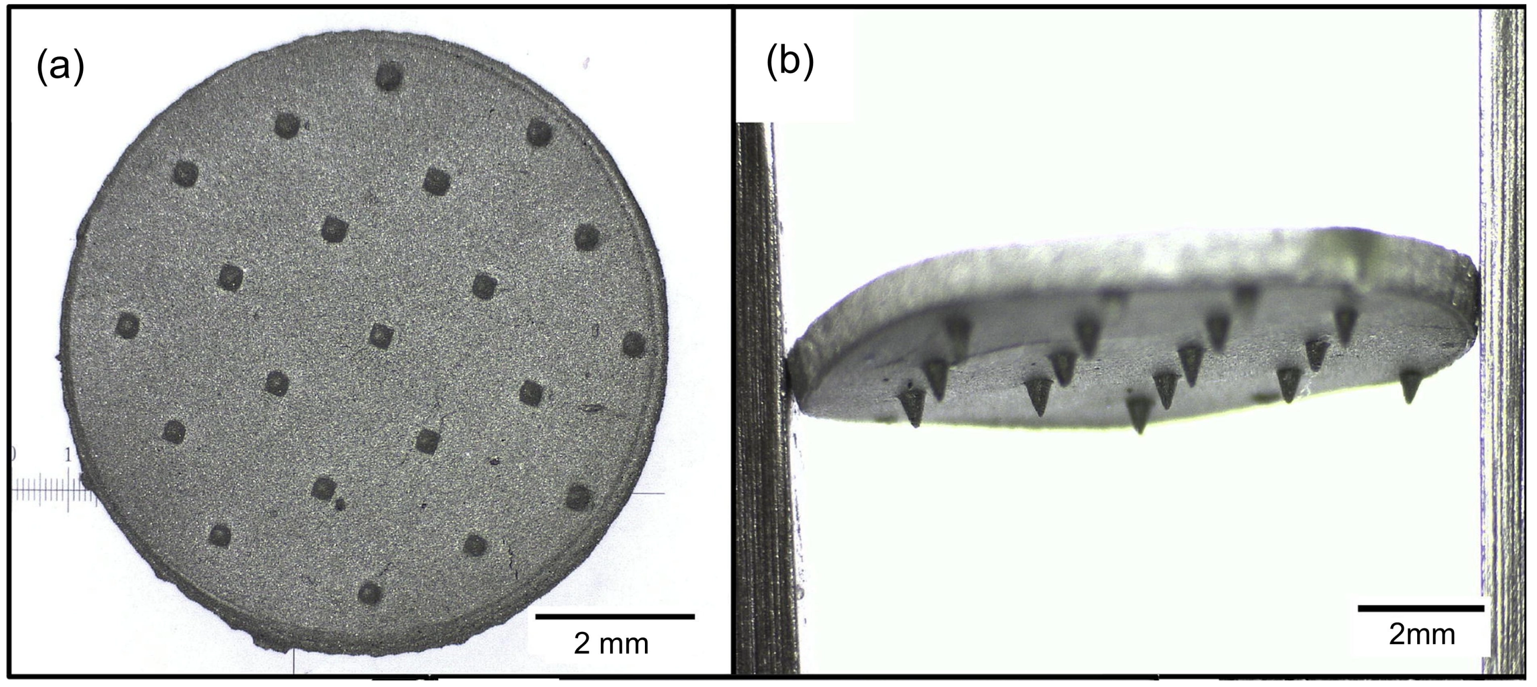
Figure 2. Finished microneedle patch under a stereo microscope. Adapted with permission from reference[20]. Copyright © 2018 Elsevier.

Figure 3. Schematic illustration of powder-based fabrication routes for CMNs. (a) Fabrication route for porous stainless-steel microneedles. Reproduced with permission from reference[20]. Copyright © 2018 Elsevier; (b) Fabrication route for flexible stainless-steel microneedle array electrodes via MLPBF. Reproduced from reference[44]. CC BY 4.0. (b - I) Tower spring inspired model; (b - II) MLPBF micrometer metal 3D printing; (b - III) Real photo and local magnification of microneedle array electrode under microscope. CMNs: conductive microneedles; MLPBF: micro laser powder bed fusion.
With the advances achieved by 316L stainless steel microneedles in terms of manufacturability and platform-level functionality, the scope of powder sintering processes has gradually expanded from specific metallic systems to a broader range of inorganic materials. Representative work by Gholami et al. demonstrated that centrifugal casting combined with high-temperature sintering can be employed to fabricate alumina microneedles with interconnected microporous networks. The resulting structures exhibited a porosity of up to approximately 60% and pore sizes in the range of 1-1.5 μm, and showed good performance in skin penetration, glucose extraction, and insulin loading and release[45]. These results indicate that powder-sintered microneedles are capable of constructing porous inorganic frameworks that can further support mass transport, surface modification, and functional integration. The core significance of this stage lies in demonstrating that the essence of powder-sintered microneedles is not restricted to specific materials, but rather represents a general manufacturing paradigm based on particle packing and the regulation of sintered pore structures. This paradigm enables the precise construction of porous frameworks at the microneedle scale, thereby providing a structural basis for subsequent surface metallization[46] and functional layer integration[47]. At this point, powder-sintered microneedles have evolved into a relatively independent fabrication route, with research focus shifting from the early feasibility of shape formation toward how to achieve synergistic control of structure and electrical properties through process parameters.
Subsequently, relevant review studies have begun to recognize powder-sintered microneedles as a relatively independent fabrication route[19], and have systematically summarized the key processing parameters involved[47]. These parameters have a direct impact on microneedle performance. For example, particle size primarily affects mold filling capability and the final pore size distribution; pore-forming agents determine porosity and pore interconnectivity; binder and solvent systems influence forming uniformity; while sintering temperature, pressure, and related conditions govern the degree of particle bonding and structural densification. From the perspective of technological development, as conventional powder forming and sintering processes have gradually matured, these methods have further extended toward metal powder-based additive manufacturing.
For example, metal powder bed fusion techniques such as laser powder bed fusion (LPBF) and its microscale variant, micro laser powder bed fusion (MLPBF), have begun to be applied in the fabrication of CMNs and related electrode structures. This development indicates that powder-based methods are evolving from traditional porous microneedle platforms toward the direct fabrication of CMNs and associated functional electrode architectures. Jiang et al. drew inspiration from the tower spring structure and designed a circular flexible microneedle array electrode composed of a multi-stage rotating cantilever beam with a serpentine cutout pattern. Using medical-grade 316L stainless steel as the feedstock, the metallic microneedle electrodes were fabricated in a single step via MLPBF. Figure 3b illustrates the microneedle array design and manufacture. This method improves fabrication resolution by employing a smaller laser spot size and a thinner powder layer thickness, thereby enabling the simultaneous formation of a lightweight flexible substrate and sharp, smooth metallic microneedles within a single processing step. The printing accuracy can reach or exceed 2 μm, with a surface roughness not higher than 0.8 μm and a tip diameter of approximately 30 μm, which is sufficient to meet the geometric requirements for skin penetration[44].
In addition, although another study did not directly fabricate standard microneedle arrays, it further demonstrated the potential of LPBF from the perspective of microscale metallic structure fabrication. In the work by Wibisono et al., gas-atomized 316L stainless steel powder was used as the feedstock. The powder was first dried, followed by layer-by-layer melting using LPBF to fabricate rectangular micropillar arrays. In their process design, the volumetric energy density and build orientation were systematically varied. The resulting structures were characterized in terms of morphology, densification, geometric accuracy, and hardness using scanning electron microscopy, optical microscopy, and Vickers hardness testing. The results showed that LPBF can directly fabricate 316L rectangular micropillar arrays with widths ranging from 200 to 800 μm. Among the tested conditions, 105 J/mm3 was identified as an optimal processing window, and structures fabricated at 0° and 45° build orientations exhibited more stable morphology, higher dimensional accuracy, and hardness values in the range of 170-220 HV[48]. Although the structures obtained in this study are still micropillar arrays rather than microneedles in the strict sense, the results demonstrate that LPBF is capable of achieving relatively stable direct fabrication of microscale metallic arrays, while exhibiting strong potential in geometric control and mechanical property tuning. This provides important methodological insights for the subsequent direct fabrication of CMNs electrodes and related three-dimensional electrode structures based on powder-based thermal processing routes. Therefore, a key shift at this stage is that powder-based methods are no longer limited to the construction of porous microneedle frameworks, but are beginning to demonstrate the capability for directly manufacturing CMNs electrodes and related functional microstructures.
3.2 Photopolymerization-based fabrication
Another important approach for the fabrication of CMNs is based on photopolymerization technologies. A representative stereolithography (SLA)-fabricated microneedle array is shown in Figure 4. Before the application of direct photopolymerization-based additive manufacturing methods, such as SLA, digital light processing (DLP), and two-photon polymerization (TPP), in microneedle fabrication, fabrication routes combining photosensitive polymer curing with microfabrication techniques were widely employed for constructing CMNs structures[50]. Early studies typically employed ultraviolet (UV) photolithography to fabricate master molds, followed by PDMS replication and polymer casting processes to obtain microneedle structures, as shown in Figure 5a.

Figure 4. Photograph of tapered MN sensor array. Reproduced from reference[49]. CC BY 4.0. MN: microneedle.
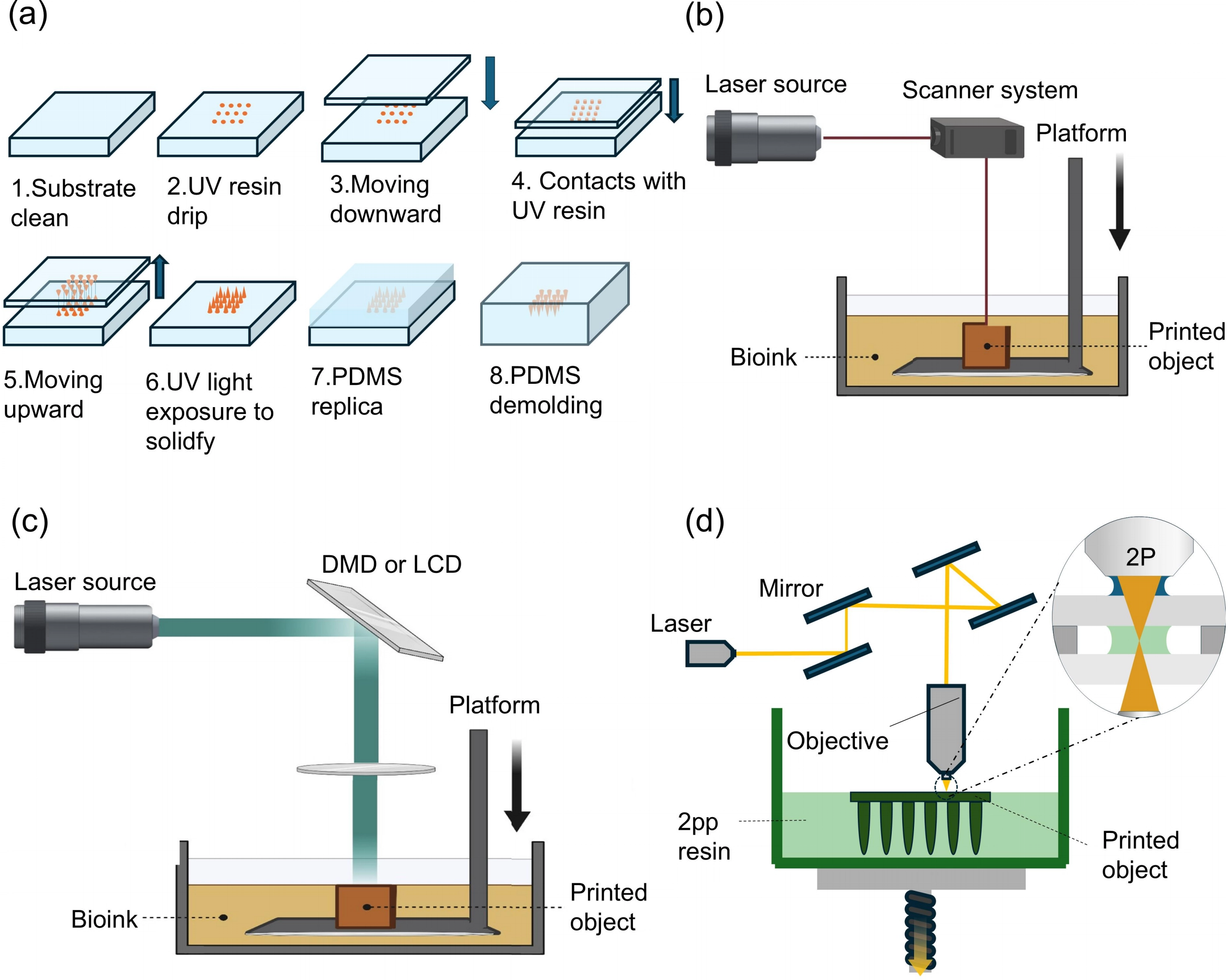
Figure 5. (a) Schematic illustration of the fabrication process for a PDMS microneedle replica mold based on UV resin patterning. Adapted with permission from reference[51]. Copyright © 2016 Springer; (b) Schematic of SLA-based fabrication. Reproduced from reference[52]. CC BY 4.0; (c) Schematic of DLP-based fabrication. Reproduced from reference[52]. CC BY 4.0; (d) Schematic of Two-photon polymerization fabrication. Reproduced from reference[53]. CC BY 4.0. PDMS: polydimethylsiloxane; UV: ultraviolet; SLA: stereolithography; DLP: digital light processing; DMD: digital micromirror device; LCD: liquid crystal display.
Lee et al. utilized a micromolding approach based on SU-8 photolithographic master molds and PDMS replica molds, combined with centrifugal casting of high-viscosity polysaccharide solutions, to fabricate dissolvable polymer microneedles. The microneedle master was formed by UV exposure of SU-8 photoresist, resulting in microneedles with lengths of approximately 600-800 μm, base widths of about 300 μm, and tip widths of around 25 μm. The resulting carboxymethyl cellulose pyramidal microneedles were able to penetrate excised porcine skin to depths of approximately 150-200 μm and could fully dissolve within 1 h, demonstrating that this approach enables high-fidelity replication of microneedle structures while allowing gentle drug loading and release[54].
Building upon this foundation, related technologies have further evolved from structural replication toward functional construction. Kim et al. adopted the basic framework of SU-8 photolithography and PDMS mold-based fabrication, but extended the material system to SU-8/Single-walled carbon nanotubes (SWCNT) conductive composites. A pressure-assisted transfer molding method was employed to achieve effective filling of high-viscosity composite materials into microneedle cavities and localized transfer molding. The fabricated microneedles exhibited a pyramidal geometry, with a height of approximately 640 μm and a base length of about 300 μm. The results showed that when the SWCNT content exceeded 0.5 wt%, the resistance of the composite microneedles could be stabilized at approximately 1 kΩ, thereby meeting the requirements for stable electrode performance. Furthermore, the surface insulating SU-8 layer was removed by inductively coupled plasma reactive ion etching (ICP-RIE) to expose the embedded SWCNT network, followed by PEDOT:PSS electrodeposition and subsequent functional layer modification. Through this process, the authors constructed an individually addressable microneedle electrode array for glucose detection[55].
This category of studies demonstrates that early microfabrication routes based on photolithographic master molds can be further extended to the construction of conductive composite microneedles and electrochemical biosensing devices, highlighting the applicability of photosensitive materials in microneedle fabrication. At the same time, research at this stage established the fundamental technical framework for subsequent photopolymerization-based microneedle fabrication and provided a material and process foundation for the development of SLA, DLP, and TPP technologies. However, although SU-8 chemically amplified photoresists were widely employed in early photolithographic micromolding processes because of their high aspect-ratio patterning capability and fabrication reliability, later studies demonstrated that alternative proprietary photocurable resins and non-SU-8 photopolymer systems could also achieve excellent structural fidelity in microneedle replication. Faraji Rad et al. reported a fabrication strategy based on non-SU-8 TPP-fabricated master molds using commercially available photocurable resin systems, coupled with reusable PDMS secondary molds and thermoplastic hot embossing for the high-fidelity replication of microneedles with open microfluidic channels[56]. This approach demonstrated that photopolymerization technologies can serve not only as direct fabrication methods, but also as ultrahigh-resolution master mold manufacturing platforms capable of producing complex three-dimensional microneedle architectures with high geometric fidelity. Nevertheless, these replication-based fabrication routes still fundamentally rely on template transfer processes, which may impose limitations on the rapid customization of dimensions, geometries, and structural architectures. In addition, many photosensitive polymers are inherently insulating, and therefore conductive functionality usually needs to be introduced through conductive filler incorporation, metallization, or other surface functionalization strategies[57-59].
In contrast to the aforementioned microfabrication routes that rely on photolithographic master molds and template replication, SLA forms structures by point-by-point curing of liquid photopolymer resins using a UV laser (Figure 5b). Owing to its high resolution, excellent surface quality, and strong geometric flexibility, SLA has increasingly become a preferred method for fabricating microstructures in conductive-enhanced polymer composite systems[35,60]. Reynoso et al. employed SLA-based direct photopolymerization printing to fabricate polymeric microneedle arrays (PMNAs), and, combined with subsequent metallization and biofunctionalization processes, constructed electrochemical biosensing microneedles for continuous drug monitoring. The authors directly printed the microneedle structures from a digital model, obtaining microneedles with a length of approximately 1.5 mm, a width of about 389 μm, and a tip size of around 65 μm, demonstrating that the SLA method can achieve microneedle fabrication with good geometric accuracy and array uniformity. Subsequently, a conductive layer was deposited on the microneedle surface via Cr/Au sputtering, followed by the introduction of an aptamer-based self-assembled interface with redox labels. In this way, the originally insulating polymer microneedles were endowed with both electrical conductivity and molecular recognition capability[49]. The significance of this work lies not only in demonstrating that SLA can be used to manufacture microneedles, but also in further revealing that its core value in CMNs fabrication resides in its role as a high-degree-of-freedom structural formation platform, which can be effectively coupled with subsequent conductive modification and biointerface functionalization processes. However, despite its advantages in geometric flexibility and fabrication precision, SLA remains fundamentally a serial fabrication technique based on point-by-point laser scanning, which may limit manufacturing throughput and increase processing time for large-area or high-density microneedle production. Therefore, SLA is currently more suitable for rapid prototyping, customized fabrication, and master mold generation, rather than direct large-scale manufacturing.
Although SLA has provided an important technical foundation for the direct digital fabrication of CMNs structures, its point-by-point curing mode still suffers from inherent limitations in manufacturing efficiency and rapid array replication. This has in turn driven the further development of DLP for conductive structure fabrication, a technique characterized by whole-layer projected exposure. DLP employs a digital micromirror device to precisely modulate the optical path through the rapid deflection of millions of micromirrors, thereby projecting patterned light onto the surface of a photosensitive resin. Unlike the point-scanning strategy used in SLA, DLP operates via planar exposure, allowing an entire layer to be cured in a single irradiation step (Figure 5c). As a result, DLP can significantly improve fabrication speed while maintaining micron-scale high resolution[61]. Lijnse et al. used DLP to fabricate low-cost conical microneedle arrays and systematically evaluated how printing parameters, needle geometry, tip sharpness, surface roughness, as well as compatibility with mold replication and coating processes influenced microneedle fabrication quality. In this study, a low-cost Sonic Mini 8K DLP printer equipped with a projection system featuring a pixel size of approximately 22 μm was used to directly print conical microneedle arrays. The fabrication behavior was further optimized by varying parameters such as needle height, aspect ratio, and layer thickness. The results showed that this approach could produce microneedle arrays with a reliability exceeding 98%, a tip curvature radius on the order of 30 μm, and sharper tip structures at lower layer thicknesses. In addition, the fabricated microneedles could serve not only as directly printed microneedles, but also as master molds for subsequent PDMS replication, while exhibiting good localized retention of drug coatings[62]. Building upon this, subsequent studies have further evolved from high-efficiency structural fabrication toward the integration of conductive devices. Wang et al. proposed a hybrid additive manufacturing strategy that combines DLP with laser-activated selective electroless plating. In this approach, a functional photosensitive resin doped with 3wt% ATO and 1wt% TiO2 nanoparticles was developed, and a three-dimensional polymer substrate was fabricated using a commercial desktop DLP printer. Subsequently, active sites were induced on the surface via a 1,064 nm near-infrared laser, followed by selective electroless copper plating to form conductive layers with a thickness of approximately 11 μm and an electrical conductivity of 5.2 × 10⁷ S/m in designated regions. Through this process, three-dimensional conformal electronic circuits were successfully constructed[63]. Taken together, these studies indicate that the DLP photopolymerization route, similar to SLA, is fundamentally based on the additive fabrication of three-dimensional substrates, followed by subsequent metallization or functionalization processes. This strategy provides a reliable and generalizable framework for the fabrication of CMNs.
While the technological evolution of SLA and DLP has largely focused on improving fabrication efficiency and processing continuity in photopolymerization-based additive manufacturing, another major direction of development has been the cross-scale advancement of spatial resolution. In this context, TPP as an ultrahigh-resolution technique with nanoscale precision, has gradually emerged as a key strategy for the fabrication of complex microneedles and high-fidelity micro/nanostructures. It is an additive manufacturing technique that utilizes laser-induced polymerization to generate three-dimensional features[64,65]. As illustrated in Figure 5d, the process begins by dropping photosensitive resin onto a glass substrate, followed by directly focusing a femtosecond laser beam onto the material. Utilizing the two-photon absorption effect as the initiation mechanism, resin curing is induced only at the laser focal point, thereby achieving point-by-point scanning forming of three-dimensional microstructures. The desired structures are formed within the bulk of the photoresist, while the unexposed regions are subsequently removed during development. Compared with other SLA-based techniques, TPP offers superior structural resolution and fidelity, as the energy and number of applied laser pulses can be precisely controlled beyond the diffraction limit[66]. Lichade et al. established a photosensitive conductive hydrogel system suitable for TPP by incorporating poly (3,4-ethylenedioxythiophene):polystyrene sulfonate, polyethylene oxide, lithium phenyl-2,4,6-trimethylbenzoylphosphinate, and glycerol, and systematically evaluated its printable window, viscosity, electrical performance, and biocompatibility. The results showed that this material could be directly processed by TPP into conductive structures such as microwires and microcapacitors, with a feature resolution of approximately 500 nm, while maintaining good structural stability and electrical performance[67].
From a manufacturing perspective, the development of photopolymerization-based CMNs fabrication strategies shares certain similarities with the evolution of microfabrication technologies in the semiconductor integrated circuit industry, where continuous trade-offs have existed between high-resolution serial fabrication and scalable parallel manufacturing approaches[68]. Serial fabrication methods, such as SLA and TPP, provide excellent geometric flexibility and structural precision through point-by-point curing or writing processes, but are often limited in throughput and large-scale manufacturability. In contrast, parallel fabrication approaches, particularly mold-based replication and embossing techniques, enable simultaneous production of large numbers of microneedles within a single processing cycle and are therefore more compatible with scalable manufacturing. Consequently, future development of photopolymerization-based CMNs fabrication may increasingly rely on combining high-resolution serial fabrication for master structure generation with scalable parallel replication strategies for practical manufacturing.
3.3 Material extrusion
Extrusion-based printing is one of the most widely used techniques in additive manufacturing, among which fused deposition modeling (FDM) represents the most fundamental and mature approach. This method primarily relies on thermoplastic polymers, which are heated to a semi-molten state and extruded through a printing nozzle according to predefined model parameters, followed by layer-by-layer deposition to form the final structure[69]. FDM offers several advantages, including low equipment cost, process maturity, and wide material availability, and has therefore been applied to the fabrication of polymeric microneedles such as those based on PLA. However, its application in microneedle fabrication is still constrained by limited printing resolution and insufficient tip fidelity, and the resulting structures often require additional optimization through chemical etching or other post-processing strategies[59].
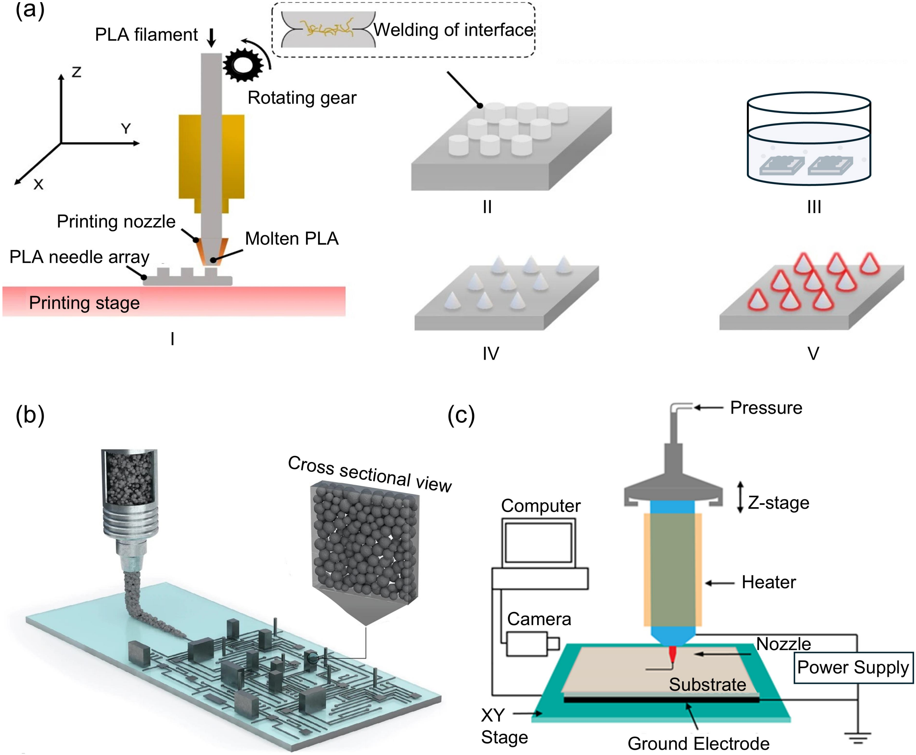
Wu et al. investigated a fabrication strategy for PLA microneedles that combines FDM with subsequent chemical etching. As shown in Figure 6a, PLA needle bodies with predefined geometries were first printed via FDM, followed by hydrolytic etching under alkaline conditions to further reduce the feature size, thereby overcoming the inherent resolution limitations of conventional FDM in producing microscale sharp tips. The authors systematically optimized key printing parameters, including nozzle temperature and build plate temperature, to enhance interlayer bonding strength and reduce internal voids, thus preventing fracture or delamination of the microneedles during the subsequent etching process. In addition, the effects of etchant concentration, temperature, and stirring conditions on the etching rate were also investigated. As a result, both straight and inclined microneedles were successfully fabricated, with lengths of approximately 1,000 μm and tip diameters of about 97 ± 21 μm and 86 ± 23 μm, respectively. The fabricated microneedles were further demonstrated to possess sufficient mechanical strength and skin penetration capability[70].

Figure 6. (a) Illustration of PLA microneedles fabricated by combining FDM and chemical etching. (a - I) PLA needle arrays with predesigned structures printed by FDM; (a - II) PLA needle arrays printed under the optimized condition to form optimal welding at the interfaces of successive layers; (a - III) PLA needles chemically etched via the hydrolysis of PLA under alkaline conditions; (a - IV) PLA microneedle array obtained after chemical etching; (a - V) PLA microneedles coated with an Active Pharmaceutical Ingredient. Reproduced from reference[70]. CC BY 4.0; (b) Schematic illustration of the PILC ink enabling 3D printed structures with high structural integrity through the dense packing of colloidal particles. Reproduced from reference[26]. CC BY 4.0; (c) Schematic of an EHD printing system. Reproduced with permission from reference[71]. Copyright © 2024 ASME. PLA: polylactic acid; FDM: fused deposition modeling; PILC: PEDOT:PSS-ionic liquid colloidal; EHD: electrohydrodynamic.
On the other hand, significant progress has been made in applying FDM to the fabrication of conductive microstructures and electrodes. Through the integration of functional materials[72,73], particularly conductive polymers and composite systems[73], the electrical conductivity and electrochemical performance of printed structures have been markedly improved. Although direct reports on the fabrication of CMNs via FDM remain limited, studies on FDM-printed conductive electrodes and microstructured electronic devices provide important supporting evidence for this approach. Tober et al. introduced thiourea-modified carbonized chitosan as a functional filler into carbon black-filled polylactic acid composite filaments and fabricated conductive electrodes via FDM. The printed electrodes achieved detection limits of 0.43 μM and 0.22 μM for dopamine and 2,4-dinitrotoluene, respectively[74]. In addition, Trindade et al. demonstrated that optimization of FDM printing parameters, including extrusion temperature, layer height, line width, and printing speed, significantly improved conductive pathway organization and electrochemical performance in PLA/carbon black electrodes. The charge-transfer resistance was reduced from 5.38 to 0.76 kΩ·cm2 after optimization, indicating enhanced electron-transfer efficiency, while the optimized electrodes achieved dopamine detection with a detection limit as low as 0.16 μmol L-1. In addition, optimization of the conductive architecture reduced the charge transfer resistance associated with layer height from 4.49 to 1.51 kΩ·cm2 and that associated with line width from 2.38 to 1.34 kΩ·cm2, demonstrating the strong influence of conductive particle distribution and interlayer organization on electrical transport behavior. These studies collectively demonstrate that both material engineering and process optimization can markedly improve the electrical conductivity and electrochemical performance of FDM-printed conductive architectures[75]. However, its application in the microneedle domain remains primarily constrained by limited printing resolution and insufficient tip precision. Although representative studies on the direct fabrication of CMNs via FDM are still scarce, existing work has validated its feasibility in both microneedle scaffold formation and the construction of conductive functional architectures. Therefore, FDM possesses a practical foundation for the fabrication of CMNs.
In contrast to melt extrusion processes based on thermoplastic filaments, direct ink writing (DIW) further expands the material scope of extrusion-based manufacturing. DIW is a layer-by-layer extrusion-based printing technique that typically involves three main steps: (1) three-dimensional modeling of the structure using computer-aided design software, (2) generation of nozzle toolpaths via slicing software, and (3) material deposition in the form of functional inks[76]. Although DIW also employs “inks” as printable feedstocks, it fundamentally differs from conventional inkjet printing in both deposition mechanism and ink rheology. In inkjet printing, low-viscosity inks are typically deposited as discrete droplets through thermal or piezoelectric actuation[77], whereas DIW relies on the continuous extrusion of viscoelastic inks under pneumatic or mechanical pressure[78]. Therefore, DIW inks generally exhibit much higher viscosities and shear-thinning behavior, enabling shape retention after deposition and supporting the fabrication of three-dimensional structures with relatively high aspect ratios. As long as the ink formulation is engineered to exhibit appropriate rheological behavior, DIW is capable of processing a wide range of materials, including conductive filler-loaded composites, conductive polymer systems, hydrogels, and various functional precursor inks[79,80]. This broad material compatibility makes DIW particularly well-suited for the fabrication of CMNs. Zhao et al. employed DIW to directly print PBS/CNT conductive composite inks onto textile substrates, resulting in conductive fabrics that exhibit combined electrical conductivity, flexibility, washability, and mechanical durability. This work demonstrates that DIW is effective for processing polymer composites containing conductive fillers, and that stable conductive structures can be achieved through the regulation of ink rheology and substrate-ink interactions[81].
Building upon this, DIW research has further evolved from conductive composite systems toward high-performance intrinsically conductive polymer inks, enabling simultaneous improvements in conductivity, resolution, and three-dimensional structural complexity while maintaining printability. Oh et al. reported a DIW conductive ink based on a PEDOT:PSS-ionic liquid colloidal system as depicted in Supplementary Figure 6b, in which centrifugal-induced dense packing of colloids was employed to achieve a conductive polymer system with high electrical conductivity, good biocompatibility, and excellent print fidelity. This ink enables printing with a resolution of approximately 50 μm and supports the fabrication of high-aspect-ratio three-dimensional structures, freestanding interconnects, and a range of implantable and epidermal bioelectronic devices. These results highlight the significant potential of DIW in the fabrication of conductive polymer-based 3D structures and complex bioelectronic systems[26]. Despite its versatility and capability for freeform fabrication, DIW still faces substantial challenges that limit its broader implementation in conductive microneedle manufacturing. To ensure smooth extrusion and shape retention after deposition, DIW inks typically require shear-thinning rheological characteristics with sufficiently high viscosity at low shear rates. However, increasing viscosity to improve filament stability and prevent structural collapse often compromises extrusion uniformity, increases printing pressure, and raises the risk of nozzle clogging[82,83]. Secondly, achieving adequate electrical conductivity generally depends on the incorporation of high concentrations of conductive fillers, but excessive filler loading can substantially alter the rheological behavior of the ink, resulting in poor flowability, unstable extrusion, particle agglomeration, and reduced printing resolution[78]. Furthermore, curing and solidification behavior also play a critical role in determining the final structural integrity and dimensional precision of printed microneedles. Improper solvent evaporation, insufficient crosslinking, or post-deposition material spreading may lead to feature distortion, tip blunting, or shrinkage-induced defects[84].
To address the inherent limitations of DIW, researchers have begun to explore manufacturing strategies driven by non-mechanical forces. Electrohydrodynamic (EHD) jet printing represents a typical high-resolution additive manufacturing technique driven by electric fields. Its working principle involves applying a high electric field between the nozzle and the substrate, inducing the formation of a Taylor cone at the nozzle tip, from which micro-nanoscale droplets or jets significantly smaller than the nozzle diameter are ejected and deposited onto the substrate[85] (Figure 6c). Compared with conventional inkjet printing, EHD jet printing offers significantly broader compatibility with ink systems, enabling the processing of a wide range of functional materials, including metals, carbon-based materials, organic semiconductors, and various polymers. The corresponding inks typically consist of functional materials, polymers, solvents, and additives.
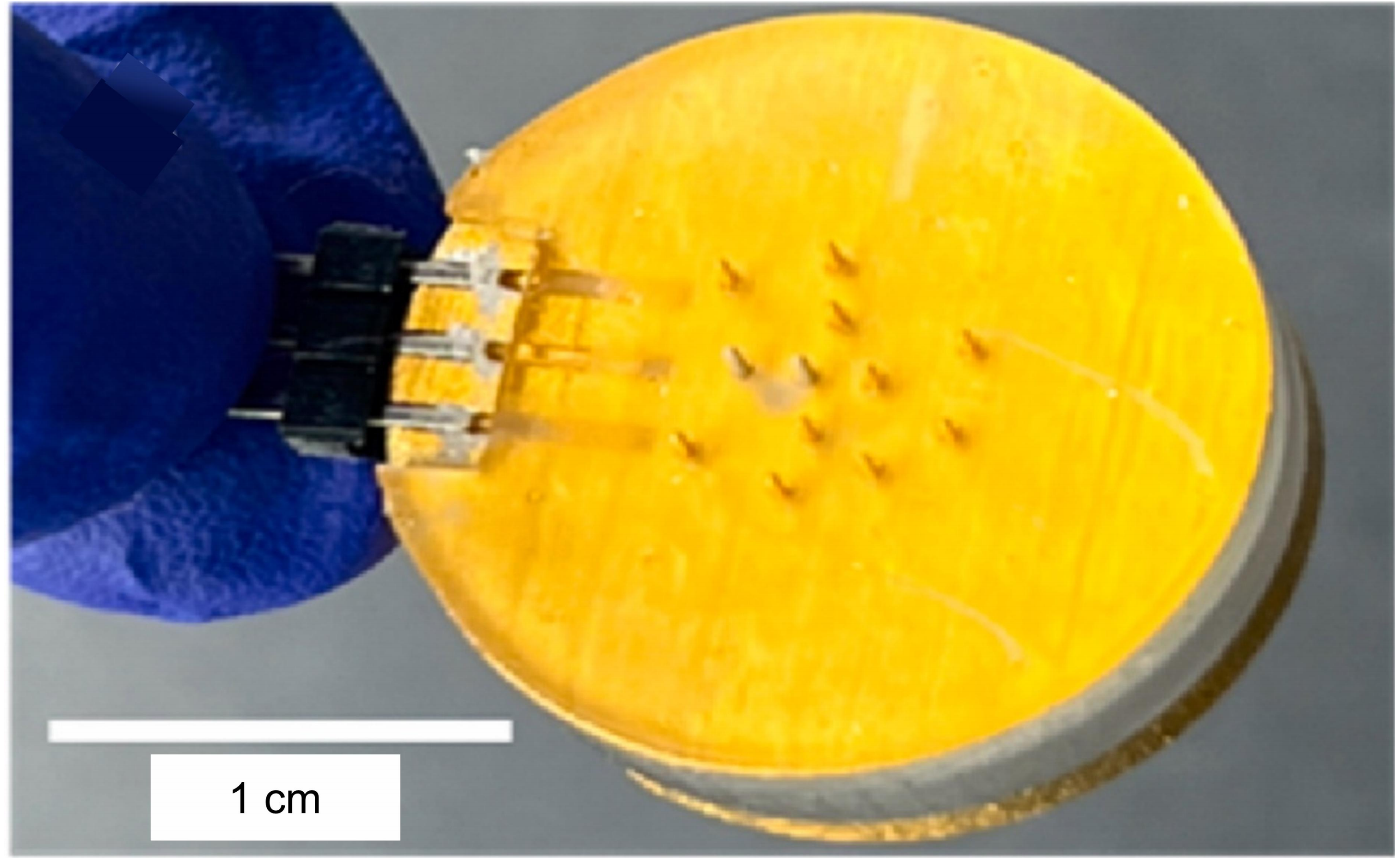
This shift in deposition mechanism not only effectively mitigates common issues in DIW, such as nozzle clogging and material spreading, but also opens new opportunities for the digital fabrication of high-aspect-ratio, ultrasharp CMNs. Gu et al. proposed a multimaterial EHD printing strategy, in which microscale conductive lines were printed using silver paste, followed by laser-assisted EHD printing of gold nanoparticles to construct three-dimensional gold pillar electrodes. The resulting gold pillars exhibited diameters as small as 0.64 ± 0.04 μm, and the devices demonstrated stable electrical conductivity, high charge storage capacity, and low impedance, enabling applications in both extracellular and intracellular electrophysiological signal recording. These results highlight the significant potential of EHD printing in the fabrication of high-resolution conductive electrodes and complex bioelectronic devices[86]. Building upon this, Wardell et al. further employed high-resolution EHD 3D printing to directly fabricate biocompatible molten alloys, successfully producing customizable three-dimensional metallic microneedle arrays. The resulting 3 × 3 microneedle arrays exhibited tunable heights in the range of 0.8-2 mm, with a minimum spacing of approximately 350 μm and a single-needle diameter of about 100 μm, as shown in Figure 7. These structures demonstrated favorable mechanical robustness, withstanding insertion into 0.6 wt.% agarose phantom tissue without bending or fracture, and exhibited excellent electrical conductivity with a resistivity of 2.096 ± 0.215 μΩ·m, enabling reliable electrophysiological signal transmission[71]. This study demonstrates that EHD is capable not only of precise deposition of conductive materials, but also of directly constructing three-dimensional metallic CMNs arrays. Compared with FDM and DIW, EHD jet printing exhibits greater potential for CMNs fabrication where high resolution, electrical functionality, and structural customizability must be simultaneously achieved. However, EHD jet printing imposes stringent requirements on jet stability and process parameter control, and still faces challenges in scalability and high-throughput manufacturing. In EHD printing, the formation and stabilization of Taylor cones rely on the application of strong electric fields, typically requiring operation under high-voltage conditions to induce and maintain stable jetting behavior[71]. Such high-voltage equipment increases system complexity, operational cost, and safety concerns compared with conventional extrusion-based printing techniques. In addition, some EHD fabrication processes may require vacuum-assisted or controlled environmental systems, which further increases equipment requirements and limits large-scale industrial implementation. Furthermore, the printing performance is highly sensitive to parameters such as voltage, nozzle-to-substrate distance, flow rate, ink conductivity, and ambient conditions, making the process difficult to standardize and scale up for industrial manufacturing. These limitations, to some extent, restrict its application in the large-area, uniform fabrication of CMNs[87].
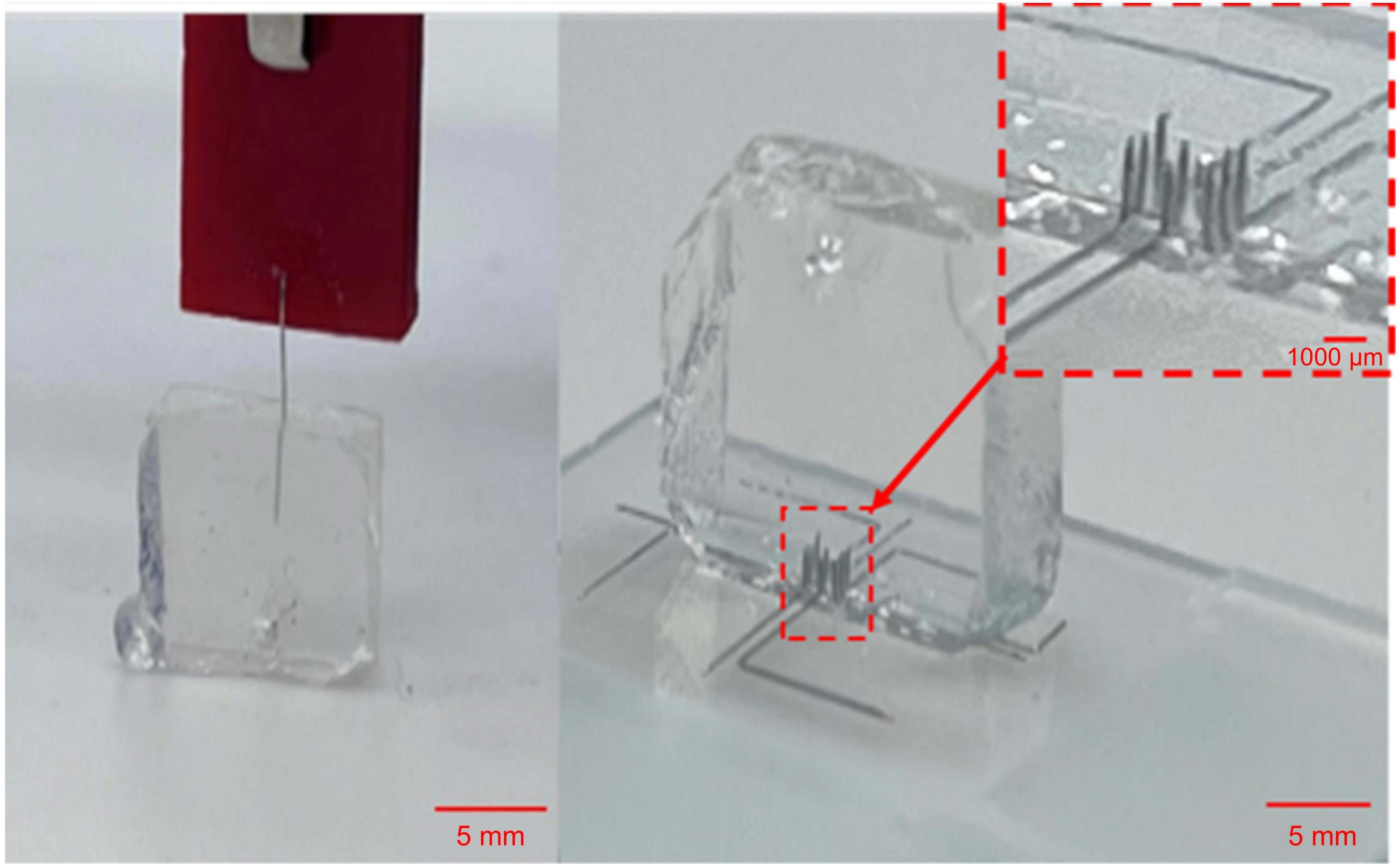
Figure 7. Photo of implantation of CMNs in phantom tissue. Reproduced with permission from reference[71]. Copyright © 2024 ASME. CMNs: conductive microneedles.
3.4 Mold-based fabrication
Mold-based fabrication remains the most mature and widely adopted technique for microneedle production, with its core principle relying on high-fidelity geometric replication to enable large-scale manufacturing of microneedle arrays. A typical mold-based fabrication process involves several steps. First, a master mold is prepared using techniques such as photolithography, micromachining, or 3D printing. This is followed by the replication of an inverse elastomeric mold, most commonly using PDMS due to its low surface energy and good stability[88]. Subsequently, the polymer precursor or drug formulation is introduced into the mold cavity, and the complete filling of the needle tip is ensured by centrifugation, vacuum-assisted filling, or pressure-assisted filling methods. Finally, after drying and demolding, the microneedle array is obtained[89-92]. In mold-based fabrication of CMNs, the formation of the microneedle structure itself is not the primary technical challenge; rather, the key difficulty lies in introducing electrical functionality after shaping. Based on the strategy used to achieve conductivity, two main approaches can be identified. The first involves fabricating non-CMNs via molding, followed by the introduction of surface conductivity through metallization, conductive coatings, or other post-processing techniques. The second approach incorporates conductive fillers directly into the composite precursor, enabling the formation of conductive composite microneedles in a single molding step. The former emphasizes the decoupling of structural formation and functionalization, allowing each to be independently optimized. In contrast, the latter focuses on the simultaneous realization of material conductivity and microneedle formation during the molding process, which is advantageous for achieving bulk conductivity throughout the needle body, but also imposes more stringent requirements on material dispersion, rheological behavior, and mold-filling performance.
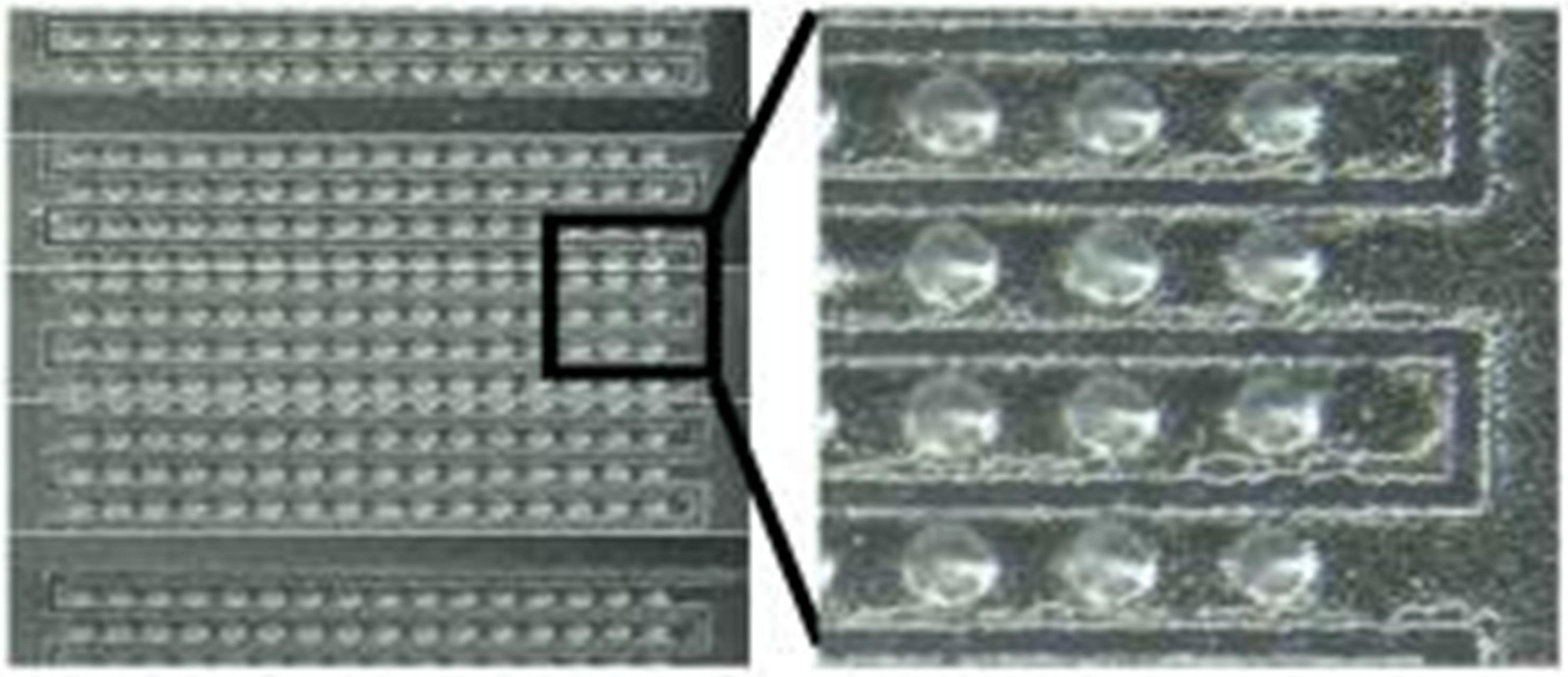
For the first approach, since structural formation and electrical functionalization are decoupled into two independent steps, this strategy is particularly suitable for surface-CMNs, bioelectrical recording electrodes, electrochemical sensing microneedles, and microneedle electrode arrays integrated with flexible substrates[93,94]. Mold-based processes enable precise optimization of structural parameters, such as tip sharpness, needle height, aspect ratio, and array uniformity, while subsequent metallization or conductive coating steps can be tailored to meet the specific electrical requirements of the intended application. In the work by Choi et al., SU-8 microneedle master molds were first fabricated using photolithography combined with reactive ion etching. The resulting structures formed a 16 × 16 array (Figure 8), with a needle height of approximately 350 μm, a base diameter of about 70 μm, and a tip curvature radius of around 3.5 μm, demonstrating good geometric precision. Subsequently, inverse PDMS molds were replicated from the SU-8 master, and poly(methyl methacrylate) (PMMA) solution was cast into the PDMS cavities. After solvent evaporation and thermal annealing, PMNAs were obtained through demolding. To introduce electrical functionality, a Ti/Cu metallic seed layer was deposited onto the PMMA microneedle surfaces, followed by laser ablation to pattern and isolate the metal layer. A Ni layer with a thickness of approximately 20 μm was then electrodeposited, resulting in electroactive microneedle electrode arrays[23]. This work is of representative significance, as it not only demonstrates the fabrication of a CMNs device, but also establishes a general design principle for mold-based CMNs, that structural replication and electrical functionalization can be decoupled and independently optimized.
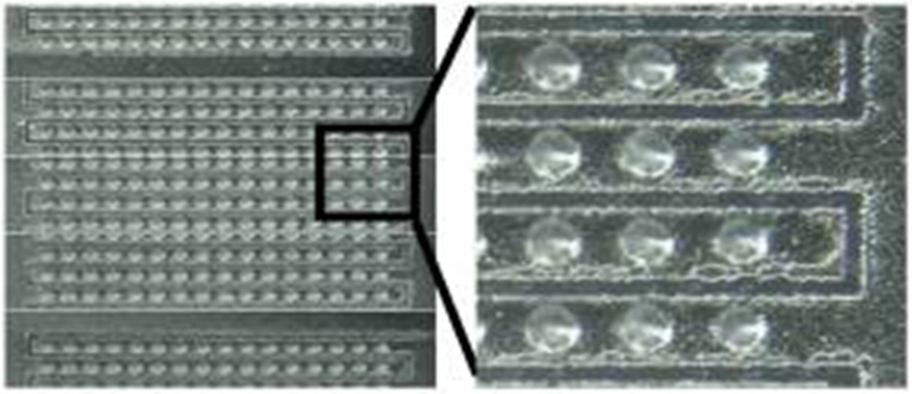
Figure 8. Optical micrograph of the fabricated 16 by 16 microneedle array. Reproduced with permission from reference[23]. Copyright © 2010 Springer.
In contrast, Jia et al. focused on the systematic optimization of metallic coatings on polymer microneedles. In their study, UV-curable polymer microneedles were fabricated using PDMS negative molds, followed by the deposition of Au thin films via magnetron sputtering. The effects of sputtering time and film thickness on surface morphology, electrical resistance, adhesion, corrosion resistance, mechanical properties, and electrochemical performance were systematically investigated. The results indicated that a sputtering time of approximately 5-6 min yields Au films with thicknesses in the range of 100-200 nm, providing optimal overall biosensing performance. Meanwhile, the metallized polymer microneedles maintained their original geometry while exhibiting enhanced mechanical properties, along with improved electrode functionality and stability[21]. Compared with earlier studies, this line of research has moved beyond the initial realization of surface metallization and basic conductivity, toward a deeper understanding of how metal layer thickness and interfacial characteristics influence mechanical insertion reliability and electrochemical sensing stability.
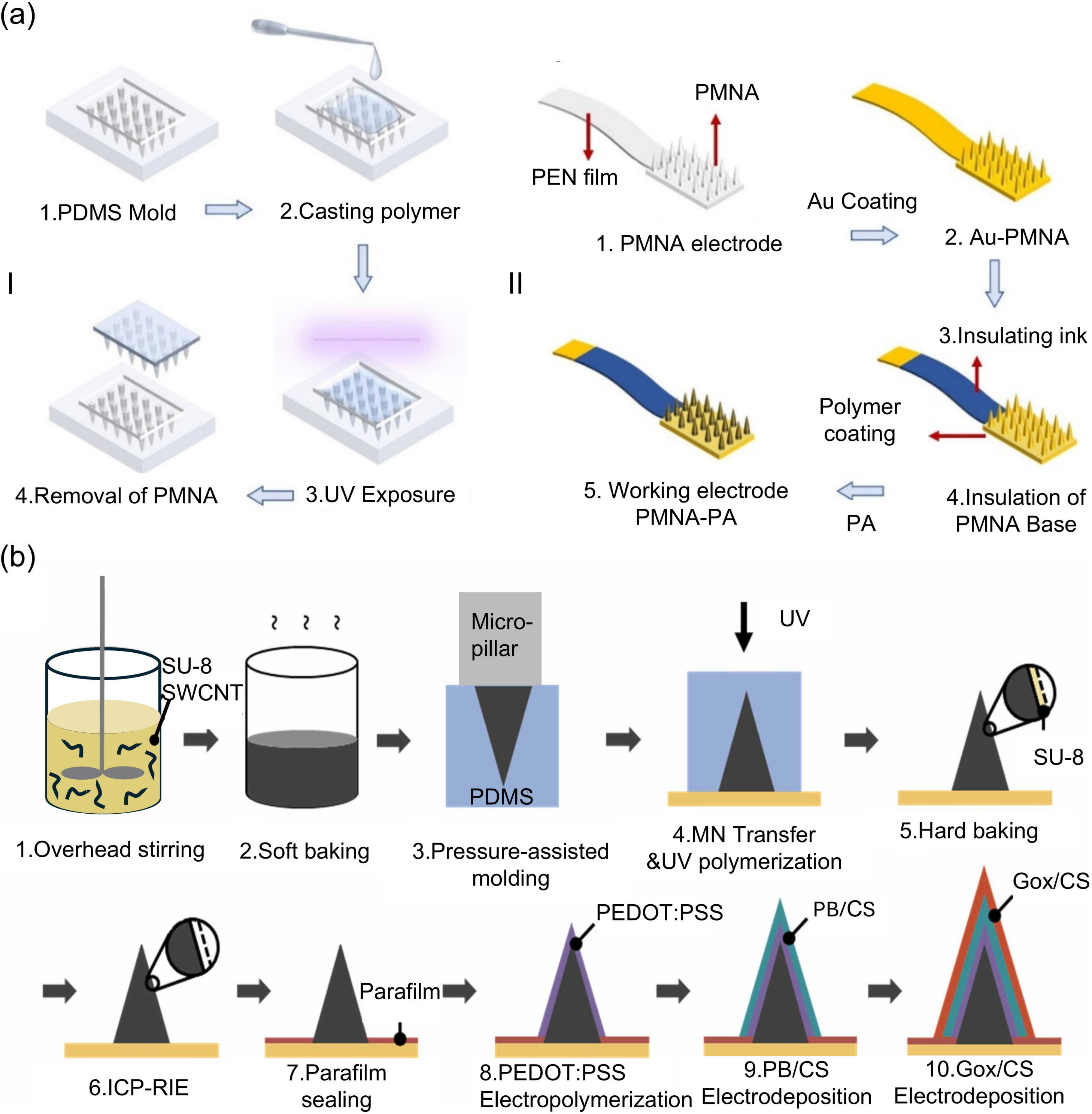
As the field has progressed, researchers have begun to exploit layered heterogeneous metal architectures to endow microneedles with multifunctionality. Rather than merely enhancing surface conductivity, strategically distributed metal layers are employed to achieve specific physicochemical functions. Dervisevic et al. introduced a heterogeneous multilayer metal system tailored to the functional differentiation of microneedle electrodes (Figure 9a). First, the PMNA was replicated from a PDMS mold by precursor casting, UV curing, and demolding. The resulting PMNA structure was then integrated onto a flexible substrate and metallized to establish electrical conductivity. Subsequently, localized insulation was introduced at the microneedle base, while the exposed electrode region was further functionalized to obtain the sensing interface. This fabrication route highlights how mold-based microneedle replication can be effectively combined with post-metallization and selective surface modification for the construction of CMNs devices[95].

Figure 9. (a) Strategies of introducing surface conductivity. Reproduced with permission from reference[95]. Copyright © 2022 Elsevier. (a - I) Fabrication process of PDMS mold and PMNA; (a - II) Fabrication process of PMNA-based electrode; (b) Fabrication scheme of composite MNs by ‘mold-and-place’. Reproduced with permission from reference[55]. Copyright © 2023 Elsevier. PDMS: polydimethylsiloxane; PMNA: polymeric microneedle array; MNs: microneedles; PEN: polyethylene naphthalate; PA: polyacrylate; UV: ultraviolet; SWCNT: single-walled carbon nanotubes; ICP-RIE: inductively coupled plasma reactive ion etching.
For the second approach, electrical conductivity is not introduced separately after microneedle formation through surface metallization. Instead, conductive fillers are pre-dispersed within the polymer matrix, endowing the material with potential electrical conductivity prior to shaping[96]. This strategy is therefore particularly suitable for bulk-CMNs, electrochemical sensing microneedles, wearable electrode-type microneedles, and integrated devices designed to simplify post-processing. Conceptually, this approach seeks to achieve both microneedle formation and conductive network construction within a single fabrication process, so that the resulting microneedles are not only conductive at the surface, but also capable of establishing continuous electrical transport pathways throughout the needle body.
In terms of material selection, the matrix typically includes thermoplastic polymers, photocurable resins, elastomers, and other biocompatible materials, while the conductive phase mainly consists of carbon-based nanomaterials, metal micro-/nanoparticles, and silver-based fillers[93,97]. By tuning the filler loading, composite systems can surpass the percolation threshold while maintaining sufficient mechanical integrity, thereby achieving effective bulk electrical conductivity. According to classical percolation theory, this threshold corresponds to the critical filler content required to form continuous electron transport pathways throughout the insulating matrix[98]. Below this threshold, conductive fillers remain electrically isolated and the composite behaves predominantly as an insulator, whereas above the threshold, conductivity increases dramatically due to the establishment of conductive pathways between adjacent fillers. For high-aspect-ratio conductive nanomaterials such as carbon nanotubes, the theoretical percolation threshold can be relatively low, owing to their large aspect ratio and high probability of network interconnection[99]. However, practical CMN systems typically require higher filler loadings to compensate for processing-induced agglomeration, non-uniform dispersion, and the need to simultaneously maintain electrochemical performance and mechanical robustness[100].
Studies have shown that conductive composite systems, exemplified by PLA/carboxyl-functionalized multi-walled carbon nanotube (PLA/f-MWCNT), can integrate the mechanical support of microneedles with electrochemical sensing functionality within a single material platform. Skaria et al. constructed PLA/f-MWCNT nanocomposite microneedles via micromolding using solution-cast composite films, achieving CNT loadings up to 6 wt% under optimized conditions. The resulting microneedles exhibited linear electrochemical responses toward ascorbic acid over the concentration range of 0.2-1 mM (R2 = 0.9282), with a detection limit of 180 μM and a sensitivity of 1.113 nA·V mM-1. In addition, the oxidation potential (~0.32 V) was significantly lower than that of conventional platinum and carbon paste electrodes, suggesting that the interconnected CNT network facilitated electron transport and improved electrochemical activity. These results demonstrate that CNT-polymer composite microneedles can simultaneously provide sufficient mechanical robustness and electrochemical functionality within a single micromolded CMN platform[97]. These results demonstrate that the incorporation of functionalized carbon nanotubes can impart electroactivity while preserving structural integrity, providing a viable pathway for constructing conductive sensing microneedles within a single-material system. Building upon this, Kim et al. further proposed a ‘mold-and-place’ strategy, extending mold-based fabrication from monolithic array replication to the construction of individually addressable electrode arrays (Figure 9b). In this approach, individual CMNs tips were first fabricated via micromolding using SU-8/SWCNT composites, followed by ICP-RIE surface treatment, and subsequently assembled one by one onto a pre-patterned electrode substrate to form an individually addressable composite microneedle electrode array, which was successfully applied for glucose sensing. Unlike the monolithic composite microneedle arrays reported by Skaria et al., this strategy decouples microneedle fabrication from electrode integration, thereby enabling mold-based methods to advance toward addressable, multi-electrode, and functionally partitioned array architectures[55].
3.5 Comparison
While the aforementioned fabrication methods demonstrate distinct advantages in terms of structural fidelity, conductivity integration, and material compatibility, their suitability for large-scale manufacturing and clinical translation varies significantly. From an engineering and translational perspective, factors such as equipment cost, processing time, and scalability for batch production are equally important when evaluating CMN fabrication strategies.
Powder-based fabrication methods provide excellent mechanical robustness and intrinsic metallic conductivity. However, these techniques generally involve high equipment costs due to the requirement for precision laser systems, inert gas protection, powder handling systems, and high-temperature processing environments. In addition, the layer-by-layer melting process is relatively time-consuming, especially for high-resolution microscale structures, which limits production throughput. Although powder-based additive manufacturing offers excellent geometric freedom and customization capability, its scalability for large-volume CMN production remains constrained by processing speed, powder recycling complexity, and operational cost.
Photopolymerization-based fabrication methods are widely recognized for their high resolution and excellent geometric fidelity. Among these techniques, SLA typically requires point-by-point laser scanning, resulting in relatively long fabrication times for large-area arrays. DLP improves manufacturing efficiency through whole-layer projection curing, thereby significantly shortening processing time and improving batch fabrication capability. In contrast, TPP offers ultrahigh nanoscale precision but suffers from extremely slow serial writing speeds and very high equipment costs associated with femtosecond laser systems, which greatly restrict its scalability for industrial production.
Extrusion-based fabrication methods generally exhibit lower equipment costs compared with photopolymerization-based manufacturing approaches. FDM systems are particularly attractive for rapid prototyping because of their affordability, simple operation, and wide availability. In addition, FDM can fabricate structures relatively quickly, making it suitable for low-cost customized manufacturing. However, its limited printing resolution and insufficient tip sharpness remain major barriers for high-performance CMNs production. DIW and EHD printing further expand material compatibility by enabling the direct deposition of conductive inks and functional composites. Nevertheless, DIW often requires careful rheological optimization and may suffer from slow printing speeds for complex arrays, while EHD printing involves relatively sophisticated electric-field control systems and stringent process parameter tuning. Although EHD can achieve exceptionally high resolution, its throughput and scalability for batch manufacturing remain limited due to jet instability and serial deposition processes.
Among current fabrication strategies, mold-based fabrication remains one of the most industrially mature and scalable approaches for CMNs manufacturing. Although the initial fabrication of high-precision master molds may involve moderate equipment costs, the subsequent replication process is relatively inexpensive and highly suitable for large-scale batch production. Furthermore, molding processes can simultaneously produce large numbers of microneedle arrays with good uniformity and reproducibility, significantly improving manufacturing throughput while reducing per-unit cost. For this reason, mold-based fabrication is considered highly promising for clinical translation and commercial manufacturing. However, additional conductive modification steps, such as metallization, conductive coating, or composite filling, may still increase process complexity and introduce potential challenges related to interfacial adhesion and long-term reliability.
A comparison of the major fabrication strategies for CMNs above is presented in Table 2.
Table 2. Comparison of different fabrication strategies.
| Fabrication strategy | Typical materials | Conductivity introduction strategy | Suitable CMNs types | Main advantages | Main limitations | Equipment cost | Processing time | Scalability for batch production | References |
| Powder-based fabrication | Metal powders, stainless steel, ceramics | Intrinsic metal conductivity or post-metallization | Porous CMNs; metallic microneedle electrodes | High strength; suitable for metallic structures | High temperature; limited material options | ***** | **** | ** | [19,47,101,102] |
| Photopolymerization-based fabrication | Photocurable resins, SU-8, polymer composites | Conductive fillers, conductive polymers, or post-metallization | Sensing microneedles; surface-conductive polymer microneedles | High resolution; sharp tips; good design flexibility | Most resins are insulating; often needs post-treatment | ** | ** | *** | [103-106] |
| Material extrusion | PLA, conductive composites, nanoparticle inks, conductive inks | Direct printing of conductive materials or composites | Bulk-CMNs; flexible CMNs | Wide material compatibility; suitable for functional materials | Limited resolution in some methods; process control can be challenging | * | *** | * | [107-110] |
| Mold-based fabrication | PDMS molds, polymers, conductive composites | Surface coating/metallization or direct molding of conductive composites | Surface-CMNs; composite CMNs | Mature process; good uniformity; scalable | Multistep processing; potential adhesion and filling issues | *** | * | ***** | [4,111-116] |
The number of asterisks (*) represents degree of each characteristic; 1 means relatively low, while 5 means high. CMNs: conductive microneedles; PLA: polylactic acid; PDMS: polydimethylsiloxane.
4. CMNs Characterizations
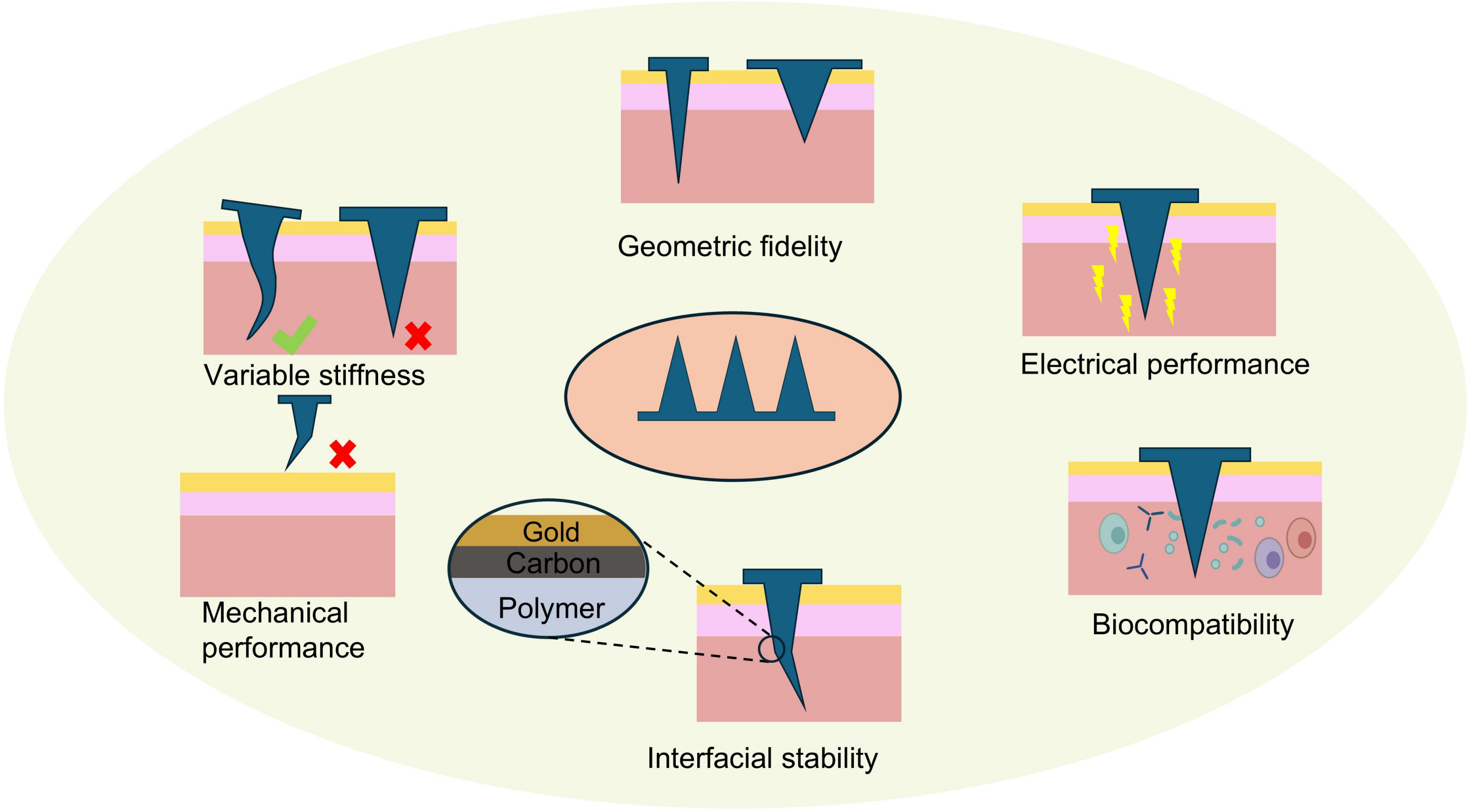
Whether a fabrication technique is truly suitable for CMNs cannot be judged solely by its ability to produce microneedle geometries or to impart electrical conductivity. More critically, it must be evaluated based on its capability to support the integrated performance required for practical device applications. From this perspective, an ideal CMNs system should simultaneously exhibit reliable mechanical support, stiffness, well-defined geometric and physical characteristics, stable electrical functionality, biocompatibility, and functional stability (Figure 10). Therefore, the assessment of different fabrication strategies should place greater emphasis on their ability to establish effective synergy among structure, material, and function.

Figure 10. Key evaluation dimensions for CMNs fabrication strategies. CMNs: conductive microneedles.
First, mechanical performance forms the fundamental basis for the functionality of CMNs. Microneedles must possess sufficient mechanical strength to prevent buckling, bending, or tip failure during skin insertion[39]. Slender microneedle geometries are generally beneficial for reducing insertion force; however, they simultaneously decrease buckling resistance, thereby increasing the risk of mechanical instability during insertion[114]. Davis et al. systematically investigated the insertion and fracture mechanics of microneedles and demonstrated that insertion force increased linearly with the microneedle tip cross-sectional area, with measured insertion forces ranging from approximately 0.08 to 3.04 N depending on needle geometry. They further showed that fracture forces could reach approximately 0.5-6 N, resulting in safety margins greater than five-fold for optimized microneedle structures[115]. In addition, the authors reported that electroplated nickel microneedles exhibited an ultimate stress of approximately 1.2 GPa and a Young’s modulus close to 200 GPa, highlighting the critical role of constituent material properties in maintaining structural robustness during insertion. Although slender microneedle geometries are beneficial for reducing insertion force, they simultaneously reduce buckling resistance and increase the risk of mechanical instability. These findings highlight the necessity of balancing insertion force requirements with buckling resistance through coordinated structural design.
Second, stiffness is another important parameter in evaluating CMNs. While strength determines whether a microneedle can resist fracture or tip failure, stiffness governs its resistance to elastic deformation. Adequate stiffness is therefore essential to maintain structural integrity and insertion reliability[116]. Recent studies have demonstrated that the mechanical stiffness of CMNs can be quantitatively tuned to balance penetration capability and tissue compliance. Zhou et al. developed a modulus-adjustable microneedle electrode in which the Young’s modulus could be regulated from 88.2 MPa to 1.98 MPa by altering the polymer composition ratio[117]. After ethanol treatment, the modulus could be further adjusted from 32.76 MPa to 1.49 MPa depending on immersion duration. Importantly, the optimized microneedles exhibited a modulus of approximately 1.98 MPa at body temperature, which closely matches the reported elastic modulus range of human skin (0.5-1.95 MPa). Such stiffness matching significantly improved conformal contact and reduced mechanical mismatch at the tissue interface. Stiffness-adaptive microneedles can combine high insertion success with improved tissue conformity, which is important for lowering irritation and enhancing long-term functional stability in applications such as sensing, stimulation, and sustained delivery. By allowing the mechanical state to change in situ, variable-stiffness designs offer a practical route to decouple penetrability from compliance, addressing a key limitation of conventional rigid or permanently soft microneedle platforms[118,119].
Third, geometric fidelity and physical characteristics play a critical role in determining microneedle insertion efficiency and penetration depth[4]. Reducing the tip curvature radius effectively lowers insertion resistance, while high-aspect-ratio structures facilitate deeper tissue penetration. In the study by Babapour et al., microneedles with a tip radius of 17.5 μm and a base radius of 150 μm achieved the greatest penetration depth, whereas those with a tip radius of 5 μm and a base radius of 200 μm exhibited the lowest penetration depth[120]. These results indicate that insertion performance is not governed solely by tip radius, but rather by the synergistic interplay among tip geometry, base dimensions, and overall aspect ratio. For CMNs, geometric fidelity not only influences penetration behavior, but also directly affects the effective electrode area, the exposure profile of conductive regions, and the reproducibility of electrochemical responses. Therefore, the capability of a fabrication method to maintain tip sharpness while achieving precise dimensional control and array uniformity constitutes a key criterion for evaluating its suitability. Beyond this, achieving sharp tip formation, fabrication methods for CMNs must also ensure dimensional consistency, array uniformity, and batch-to-batch reproducibility, particularly for applications requiring stable sensing and bioelectrical interfacing.
In addition, electrical performance constitutes the defining characteristic that distinguishes CMNs from conventional microneedles. An ideal CMNs should not only possess intrinsic electrical conductivity, but also establish continuous, stable conductive pathways tailored to the requirements of the target application. In bioelectrical recording applications, maintaining stable electrical performance under dynamic mechanical conditions is particularly important because electrophysiological signals are typically characterized by low current amplitudes and are highly susceptible to electrical noise and impedance fluctuations[121]. In conductive composite CMNs based on percolative conductive networks, mechanical deformation may alter the contact state and tunneling distance between adjacent conductive fillers, thereby affecting conductive pathway continuity and signal stability[100]. For example, Yun et al. demonstrated that the conductivity of a hybrid conductive composite increased from an insulating state to 231.2 S·m-1 under a compressive stress of 120 kPa due to deformation-induced conductive network rearrangement[122]. Such electromechanical coupling effects may lead to resistance drift, motion-induced signal artifacts, and fluctuations in interfacial impedance during long-term operation. Therefore, beyond achieving initial conductivity, conductive CMNs intended for electrophysiological recording should also maintain stable conductive network integrity and reliable electrode–tissue interfacing under repeated mechanical deformation and prolonged wear conditions.
Finally, beyond the aforementioned performance metrics, biocompatibility, interfacial adhesion, and functional stability are equally critical considerations. CMNs are typically employed in applications such as biosensing[123], disease monitoring[124], electrophysiological recording[125], transdermal drug delivery[126], and stimulation-based therapies[113]. Given their direct interaction with the skin, interstitial fluid, and even deeper tissues, their operation inevitably involves potential risks of immune response and tissue damage, necessitating systematic evaluation of biocompatibility and long-term safety. For instance, Li et al. developed a bioresorbable electrochemical microneedle sensor array that demonstrated stable in vivo operation with minimal tissue damage and favorable biosafety profiles, as verified by histological and blood biochemical analyses. In addition, the implanted device could gradually biodegrade after use, thereby avoiding secondary surgical retrieval and reducing additional tissue trauma[127]. For CMNs systems based on surface modification, the interfacial adhesion between the conductive layer and the substrate is a key determinant of structural integrity and functional stability. Coating cracking, delamination, or degradation of conductive networks may lead to deteriorated electrical performance or even device failure.
Taken together, these characterization dimensions are highly interdependent in practical CMNs design. In particular, electrical conductivity and mechanical reliability often exhibit competing relationships in conductive composite systems and surface-functionalized microneedles. Increasing conductive filler loading or introducing conductive coatings can improve electrical performance, but may simultaneously compromise stiffness, fracture resistance, tip fidelity, or long-term structural stability. Therefore, balancing conductivity and mechanical robustness has become one of the central considerations in CMNs fabrication and application design. The electrical and mechanical properties of representative CMNs prepared by different fabrication strategies are summarized in Table 3.
Table 3. Electrical and mechanical properties of representative CMN.
| Fabrication strategy | Representative studies | Electrical performance | Mechanical performance | Aspect Ratio | References |
| Powder-based fabrication | 316L stainless steel microneedle | 1.4 × 10⁶ S/m | withstand ~19 N insertion load | 1.13 | [45] |
| Powder-based fabrication | Flexible 316L stainless steel microelectrode | Impedance: ~3-4 kΩ | Penetration rate: 98.3% | 2.5 | [44] |
| Photopolymerization-based fabrication | Cu-plated DLP photopolymer microneedle | 5.2 × 10⁷ S/m | Tensile strength: 23.37 ± 0.25 MPa | 3.9 | [49] |
| Photopolymerization-based fabrication | PEDOT:PSS-coated SLA microneedles | Sheet resistance: 324 ± 2 Ω sq-1 | Penetration displacement: 54.7 ± 3.19 μm at 0.08 N/needle | 2.4 | [128] |
| Material extrusion | Sub-microscale 3D gold pillar bioelectrode | 97.14 ± 51.39 MΩ at 1 kHz | Bending stiffness: 3.86 N μm-3 | 7.8 | [86] |
| Material extrusion | Ag nanoparticle inkjet-printed microneedles | Resistance: 110 mΩ | Young’s modulus: 15.6 GPa; hardness: 0.24 GPa | 5 | [129] |
| Mold-based fabrication | Bismuth-Indium-Tin alloys electrode | Electrode-skin impedance < 10 kΩ after penetration | 0.09 N/needle | 2.35 | [130] |
| Mold-based fabrication | Gold ink-casted Au microneedles | Sensitivity: 31 nA/mM | Fracture force: 30 ± 2 N | 1.54 | [131] |
CMN: conductive microneedle; DLP: digital light processing; SLA: stereolithography.
5. Applications
Microneedles have been widely applied in areas such as biosensing, bioelectrical signal acquisition, electrostimulation therapy, and electrically controlled drug delivery, and have gradually evolved into an important transdermal bioelectronic interface (Figure 11).
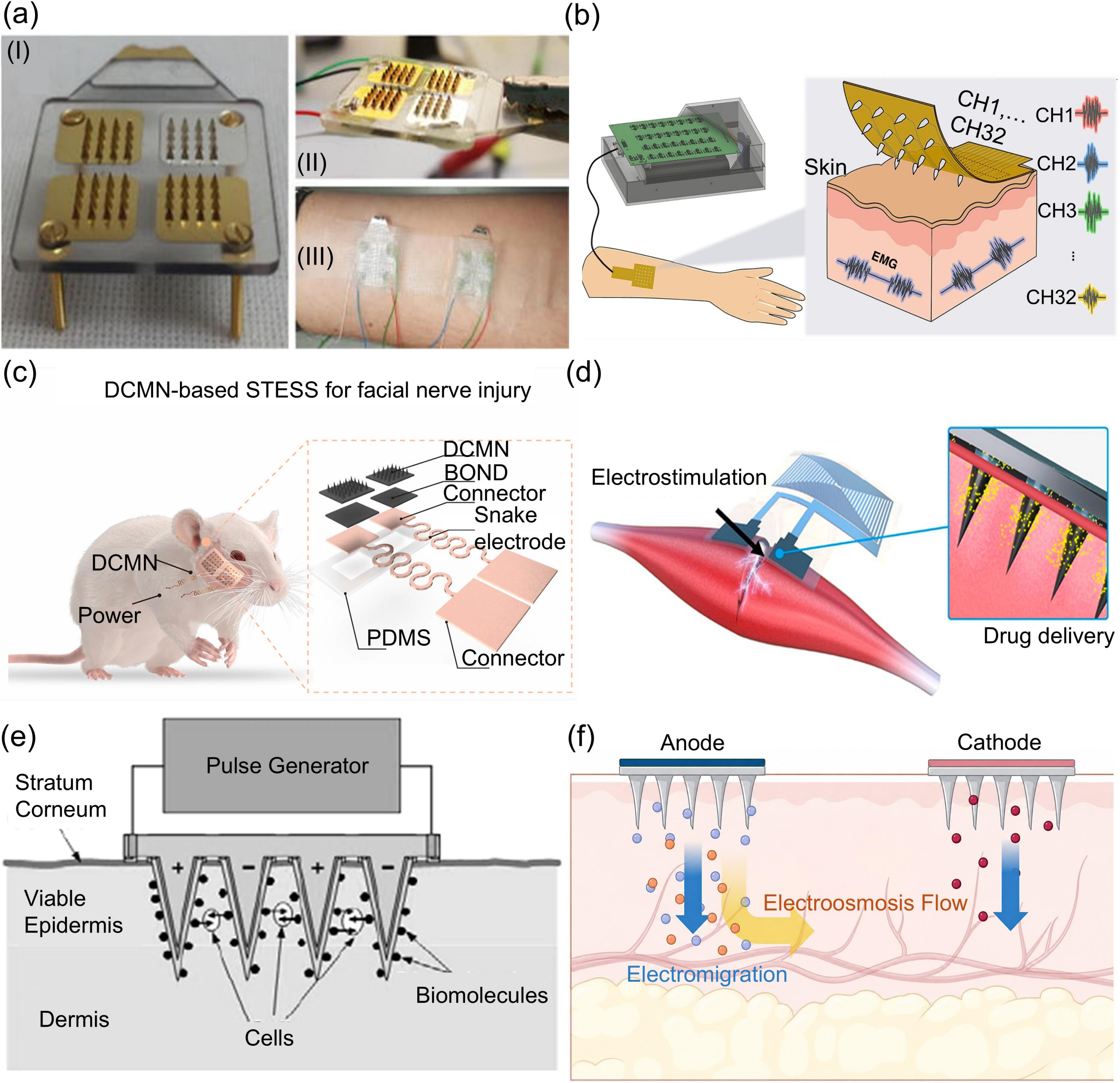
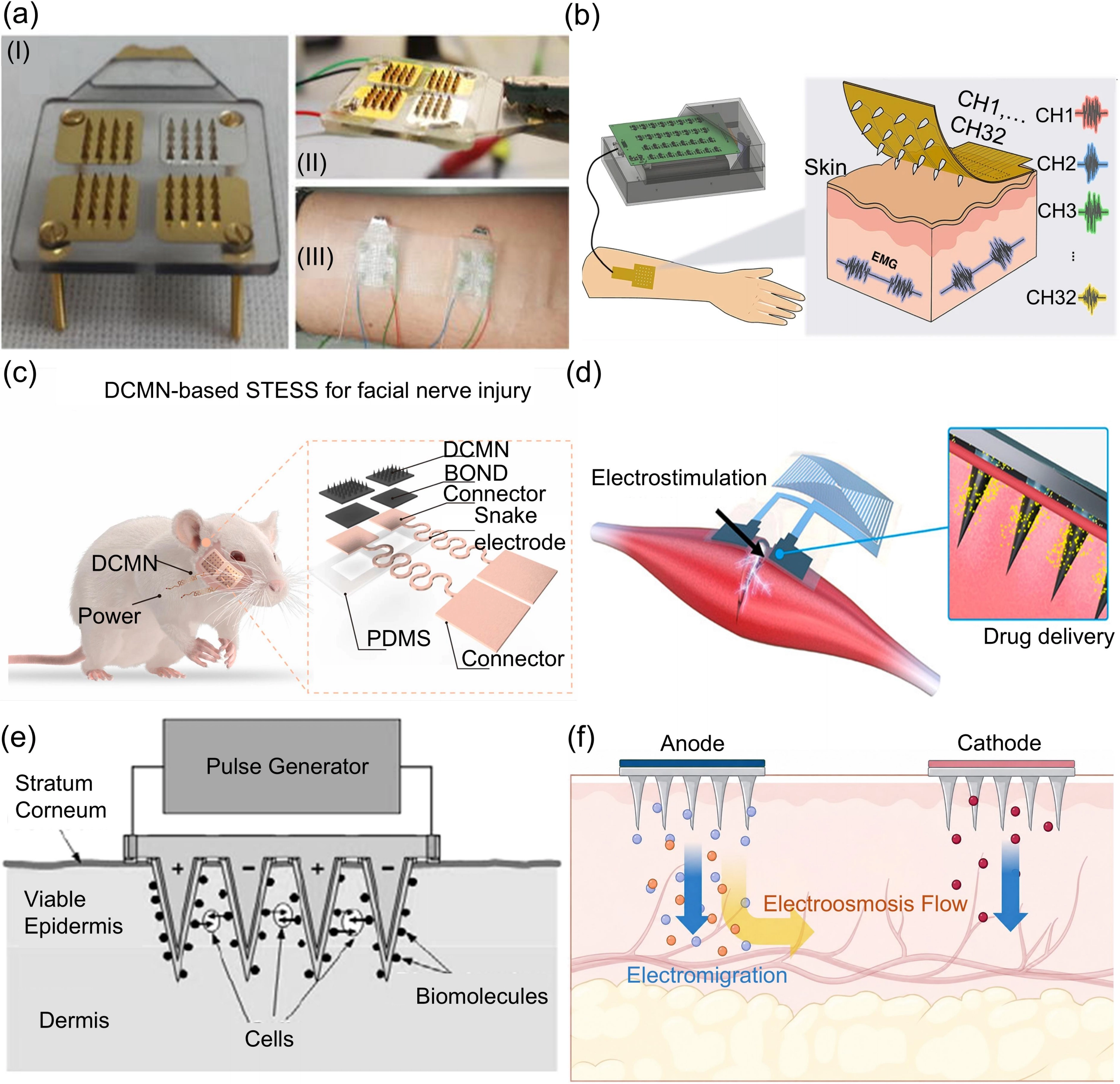
Figure 11. (a) A coated microneedle sensing device for continuous in vivo molecular monitoring. (a - I) unfunctionalized microneedle patch; (a - II) patch functionalized on three gold working electrodes; (a - III) two patches applied to an arm. Reproduced from reference[132]. CC BY 4.0; (b) Real-time EMG signal detection via a microneedle array sensor worn on the arm. Reproduced from reference[133]. CC BY 4.0; (c) Electrical stimulation treatment of facial paralysis rats by a DCMN-based method. Adapted from reference[134]. CC BY 4.0; (d) Electrically controlled drug delivery. Reproduced with permission from reference[135]. Copyright © 2022 American Chemical Society; (e) Electroporation-enabled intracellular delivery using conductive microneedles. Reproduced with permission from reference[23]. Copyright © 2010 Springer; (f) Schematic illustration of mechanisms of iontophoresis-assisted transdermal delivery. Reproduced from reference[136]. CC BY 4.0. EMG: electromyography; DCMN: dissolvable CMNs; PDMS: polydimethylsiloxane.
5.1 Electrochemical biosensing
Electrochemical biosensing has emerged as one of the most important application directions for CMNs, primarily because conventional biofluid analysis methods are typically invasive and remain challenging for continuous, real-time, and long-term wearable monitoring[4]. In contrast, CMNs enable minimally invasive access to interstitial fluid while simultaneously serving as electrochemical interfaces, thereby analyzing real-time biomolecular information, improving patient comfort, and enhancing compatibility with wearable platforms. Dervisevic et al. developed a wearable surface-conductive polymer CMN array fabricated via mold-based replication followed by metallization and surface functionalization for monitoring pH in interstitial fluid, demonstrating the feasibility of continuous transdermal electrochemical analysis under wearable conditions[95] (Figure 11a). Then, the same research group reported a wearable microneedle patch for urea monitoring, in which recessed microcavities were introduced to prevent delamination of the sensing layer during skin insertion. The device exhibited high sensitivity and selectivity, with a linear detection range of 3-18 mM, highlighting the importance of synergistic optimization between structural design and electrochemical functionality in CMN-based biosensors[94]. Later, they further developed a high-density wearable electrochemical microneedle biosensor for insulin detection in interstitial fluid, achieving selective quantification within a range of 0.01-4 nM. This work underscores the significant potential of CMNs in hormone monitoring and precision medicine applications[137]. Recently, Chang et al. reported a hybrid flexible wristband platform that integrates multiplexed microneedle biosensors with ultrasonic transducers[138]. This system enables the concurrent monitoring of interstitial fluid biomarkers, such as glucose, lactate, and alcohol, as well as critical cardiovascular parameters including blood pressure, arterial stiffness, and heart rate. As a pioneering effort, this study represents the first integration of a microneedle array with an ultrasound sensor on a single wearable wristband, facilitating continuous, multimodal tracking of metabolic and hemodynamic signals. Collectively, these advancements illustrate the evolution of CMNs from standalone electroactive microstructures into sophisticated, integrated biosensing platforms capable of minimally invasive, real-time, and wearable health surveillance.
5.2 Bioelectric signal acquisition
In the field of bioelectrical signal acquisition, CMNs can function as minimally invasive dry electrodes for obtaining stable electrophysiological signals. Conventional wet electrodes rely on conductive gels, which are prone to dehydration-induced impedance fluctuations and may cause skin irritation, while traditional dry electrodes are limited by the high-resistance stratum corneum, resulting in elevated interface impedance. Microneedles are therefore regarded as an ideal platform for the development of advanced biosensing devices[139]. By leveraging their microscale dimensions to bypass the high-impedance barrier of the stratum corneum, CMNs establish a compact electrode-tissue interface, thereby ensuring improved signal stability and consistency. From the perspective of technological evolution, CMNs not only realize the recording of signals, but also solve the core contradiction of obtaining low-noise and long-range signals without auxiliary media in flexible bioelectronics. Accordingly, microneedle arrays hold significant strategic value for next generation wearable electrophysiological monitoring systems. Liu et al. developed a multichannel metal-coated dry-electrode CMNs patch fabricated via micromolding and conductive surface metallization for the painless transdermal acquisition of various bioelectrical signals, including electrocardiography, electromyography, and electroencephalography[133] (Figure 11b). This study not only proves that CMNs can obtain high-quality signals in different electrophysiological scenarios, but also proves that microneedle electrodes are no longer limited to single-point low-impedance contact, but have begun to develop in the direction of multi-channel, system-level, and wearable integration, providing a new technical path for the next generation of long-term electrophysiological monitoring devices.
5.3 Electrostimulation and neuromodulation
As a minimally invasive electrode interface, CMNs overcome the limitations of conventional surface electrodes with high impedance and deeply penetrating electrodes associated with significant tissue damage. By integrating conductive materials, CMNs can penetrate the high-resistance stratum corneum and establish low-impedance contact with dermal tissues or peripheral nerves. This efficient charge transfer capability enables microneedle arrays to induce localized electric fields at low applied voltages, thereby precisely triggering cellular physiological responses or modulating neuronal activity, offering new therapeutic strategies for chronic pain management and localized functional recovery. Through the delivery of controlled electrical stimuli, CMNs can be used to promote electro-healing of deep tissues (Figure 11c), and can be applied to the repair of diabetic wounds and the treatment of nerve damage, among other applications. With the development of CMNs electrodes and closed-loop treatment systems, these devices are gradually expanding into the areas of neuromodulation and neuro-related therapies. For example, Li et al. developed an integrated self-powered conductive composite dissolvable microneedle device fabricated via mold-based casting that delivers tannic acid and zinc ions across the skin barrier while simultaneously electrically stimulating infected diabetic wounds, thereby reducing oxidative stress, inhibiting bacterial infection, and accelerating tissue regeneration[140]. Furthermore, when integrated with biosensing capabilities, CMNs can dynamically adjust electrical stimulation parameters based on real-time physiological signals, enabling intelligent and precise neuromodulation[113].
5.4 Drug delivery and electrically controlled release
By modulating externally applied electrical parameters, such as voltage amplitude, pulse frequency, and duration, researchers can precisely control the release rate and dosage of drugs within microneedle matrices (Figure 11d), thereby overcoming the pronounced initial burst release and insufficient sustained dosing commonly associated with conventional microneedle systems. In clinical applications, electrically controlled microneedles have demonstrated significant potential in areas such as on-demand insulin delivery, localized chemotherapy, and patient-controlled analgesia. When integrated with flexible electronic systems, CMNs can trigger drug release in response to real-time physiological cues, such as glucose levels or inflammatory biomarker concentrations. This approach not only improves drug utilization efficiency but also reduces systemic toxicity and side effects. Qi et al. developed an electrically responsive CMNs system based on thiolated silk fibroin and graphene, fabricated through mold-based polymer casting, for the controlled transdermal delivery of insulin[141]. In this system, electrical stimulation induces the cleavage of disulfide crosslinks and enhances microneedle swelling, thereby accelerating insulin release. Upon removal of the stimulus, the crosslinks are restored, leading to a reduced release rate and enabling a reversible “on-off” electrically controlled release behavior. Experimental results demonstrated that the microneedles exhibited a higher insulin release rate and improved in vivo glycemic control under electrical stimulation. In diabetic animal models, blood glucose levels were maintained within a safe range for up to 11 h, highlighting the significant potential of CMNs in intelligent transdermal drug delivery and closed-loop therapeutic systems.
5.5 Electroporation-assisted transdermal delivery
Electroporation is an electrically mediated strategy that transiently increases cell membrane and skin barrier permeability by applying short electric pulses[142]. When combined with microneedle platforms (Figure 11e), electroporation can further enhance transdermal transport by coupling the physical microchannels created by microneedles with electrically induced permeabilization[143]. In this context, conductive microneedles are particularly attractive because they can act not only as penetration elements but also as localized microelectrodes for delivering electric pulses directly within or near the skin. This localized electric-field distribution may reduce the required voltage compared with conventional surface electrodes and improve delivery efficiency for macromolecules, nucleic acids, vaccines, and other therapeutics with limited passive skin permeability. Therefore, CMNs-assisted electroporation provides a promising route for electrically enhanced transdermal delivery and minimally invasive therapeutic administration.
5.6 Iontophoresis-assisted transdermal delivery
Unlike electrically controlled release systems that regulate drug liberation from responsive microneedle matrices, iontophoresis-assisted delivery primarily relies on electrically driven molecular transport across biological tissues. It uses a low-intensity electric current to promote the migration of charged molecules across the skin (Figure 11f). Compared with passive diffusion-based microneedle delivery, iontophoresis provides an additional driving force for controlled and directional molecular transport[144,145]. The integration of conductive microneedles with iontophoretic systems can shorten the ion transport pathway by bypassing the stratum corneum and establishing direct electrical contact with the viable epidermis or superficial dermis. This design may enhance delivery efficiency, reduce skin impedance, and enable more precise control over dosing through the regulation of current intensity and stimulation duration. As a result, CMN-based iontophoresis represents a valuable extension of electrically controlled drug delivery, particularly for charged drugs, peptides, proteins, and other bioactive molecules.
6. Conclusion and Perspectives
6.1 Summary
This review provides a comprehensive overview of recent advances in the fabrication, characterization, and application of CMNs. As an emerging class of transdermal bioelectronic devices, CMNs combine the minimally invasive nature of microneedle systems with the electrical functionalities required for biosensing, bioelectrical signal acquisition, electrical stimulation, and electrically controlled drug delivery. This work systematically summarizes the major fabrication strategies for CMNs, including powder-based methods, photopolymerization-based techniques, material extrusion approaches, and mold-based fabrication. Particular emphasis is placed on their forming mechanisms, material compatibility, advantages, and inherent limitations. In addition, the key characterization dimensions of CMNs, including mechanical performance, stiffness, geometric fidelity, electrical functionality, and biocompatibility, are discussed, highlighting the importance of synergistically balancing structure, material, and function for practical applications. Representative applications of CMNs in sensing, recording, stimulation, and drug delivery are also reviewed, demonstrating their potential as multifunctional bioelectronic platforms. Despite these advances, several challenges remain, including fabrication precision, the trade-off between mechanical and electrical performance, material stability, and the translation from laboratory-scale demonstrations to practical applications. Overall, continued progress in fabrication techniques, conductive material design, and device-level integration is expected to further advance CMNs toward more reliable, application-oriented systems.
6.2 Challenges and perspectives
Despite the rapid progress in the field of CMNs, several challenges still constrain its further development. Improving fabrication precision and ensuring stability under complex operating conditions are critical for advancing microneedle manufacturing technologies. For CMNs, geometric precision not only influences insertion behavior, but also directly affects the effective electrode area, interfacial impedance, and electrochemical response. In the case of surface-metallized or multilayered microneedles, insufficient interfacial adhesion may lead to film delamination or functional failure during operation[146,147].
Variable-stiffness microneedles have emerged as a promising strategy to reconcile the conflicting requirements of high insertion stiffness and post-insertion mechanical compliance. Recent approaches, including phase-change materials[148], swelling hydrogels[149], and stimuli-responsive polymer systems[150], have demonstrated the ability to dynamically modulate mechanical properties after skin penetration. In particular, hydrogel-forming microneedles can significantly soften upon water absorption and swelling, thereby reducing mechanical mismatch with biological tissues, while phase-transition materials enable reversible stiffness regulation under external stimuli.
However, integrating such variable-stiffness mechanisms into CMNs remains highly challenging. Swelling-induced deformation may disrupt conductive pathways or induce delamination of conductive coatings, resulting in unstable electrical performance. Similarly, phase-transition processes may compromise the integrity of conductive networks and interfacial stability. Moreover, conductive fillers and coatings often increase structural rigidity and restrict the modulus-transition capability of adaptive materials. Consequently, achieving simultaneous optimization of conductivity, dynamic mechanical adaptability, and reliable insertion behavior remains difficult. Future efforts should therefore focus on multifunctional material systems and fabrication strategies capable of integrating stable conductive networks with controllable stiffness-transition behavior, thereby enabling CMNs with improved biomechanical compatibility and long-term functional reliability.
From a broader perspective, the rapid development of AI-driven decoding and bio-integrated robotics is expected to create new opportunities for CMNs. In particular, CMNs with high aspect ratios may enable access to deeper tissue regions and provide richer electrophysiological and biochemical information with improved spatial resolution. Such high-dimensional and continuously acquired datasets could serve as valuable inputs for machine-learning-assisted physiological decoding, intelligent prosthetic control, and closed-loop bioelectronic systems, which in turn place increasingly stringent requirements on the quality, stability, and noise characteristics of the acquired physiological signals.
As these emerging systems increasingly rely on continuous, accurate, and low-noise physiological data, CMNs will need to provide high-quality and stable signal interfaces rather than merely achieving basic tissue penetration. In particular, future studies should place greater emphasis on systematically characterizing key electrical performance parameters, such as interfacial impedance stability (< 5 - 10 kΩ)[151], SNR (> 20 dB)[152], resistance drift (< 5%)[153], and motion-induced signal artifacts under dynamic mechanical conditions, since these factors critically influence the reliability of long-term bioelectrical recording. Under this trend, high conductivity, low impedance, and long-term interfacial stability will become key performance targets for future device design.
In this context, emerging bioelectronic materials and electrically gated sensing architectures may provide additional opportunities for the next generation of CMNs systems. Recent advances in two-dimensional semiconductor materials, such as graphene and transition metal dichalcogenides, have demonstrated excellent electrical conductivity, high carrier mobility, tunable electronic properties, and strong sensitivity toward biomolecular interactions in field-effect transistor-based biosensors[154,155]. These materials have shown significant potential for point-of-care diagnostics, real-time biochemical monitoring, and wearable bioelectronics. The integration of such low-dimensional conductive materials with CMNs platforms may further improve signal transduction efficiency, reduce interfacial impedance, and enhance the sensitivity and stability of transdermal bioelectronic interfaces. Nevertheless, challenges including material biocompatibility, long-term operational stability, scalable fabrication, and reliable integration with flexible microneedle structures still need to be systematically addressed.
Finally, most CMNs systems remain at the prototype stage, and substantial efforts are still required to facilitate their translation into practical applications. Future development should focus not only on the fabrication of CMNs themselves, but also on their integration with flexible electronics, sensing modules, on-demand drug delivery, and closed-loop therapeutic platforms. In parallel, the field still lacks standardized evaluation frameworks for electrical performance, interfacial reliability, and biosafety. Addressing these issues will be essential for moving CMNs from laboratory demonstrations toward robust and manufacturable bioelectronic systems.
Acknowledgements
ChatGPT (OpenAI, GPT-5.5) was used solely for language editing and polishing of the manuscript. The authors take full responsibility for the integrity, accuracy, and originality of the content.
Authors contribution
Zhang QT: Supervision, writing-review & editing.
Zhang Q: Writing-original draft.
Tang SY: Conceptualization, writing-review & editing.
Wu L, Gaira S, Lai J, Wang R, Zhao Y: Writing-review & editing.
Conflicts of interest
The authors declare no conflicts of interest.
Ethical approval
Not applicable.
Consent to participate
Not applicable.
Consent for publication
Not applicable.
Availability of data and materials
Not applicable.
Funding
The work was funded by the Australian Research Council Future Fellowship (Grant No. FT230100257), Discovery Project (Grant No. DP250103029), and UNSW Scientia Fellowship (This program does not have a grant number).
Copyright
© The Author(s) 2026.
References
-
1. Wu C, Yu Q, Huang C, Li F, Zhang L, Zhu D. Microneedles as transdermal drug delivery system for enhancing skin disease treatment. Acta Pharm Sin B. 2024;14(12):5161-5180.[DOI]
-
2. Aldawood FK, Andar A, Desai S. A comprehensive review of microneedles: Types, materials, processes, characterizations and applications. Polymers. 2021;13(16):2815.[DOI]
-
3. Wu Z, Qiao Z, Chen S, Fan S, Liu Y, Qi J, et al. Interstitial fluid-based wearable biosensors for minimally invasive healthcare and biomedical applications. Commun Mater. 2024;5:33.[DOI]
-
4. Kim G, Ahn H, Chaj Ulloa J, Gao W. Microneedle sensors for dermal interstitial fluid analysis. Med X. 2024;2:15.[DOI]
-
5. Tang X, Dong Y, Li Q, Liu Z, Yan N, Li Y, et al. Using microneedle array electrodes for non-invasive electrophysiological signal acquisition and sensory feedback evoking. Front Bioeng Biotechnol. 2023;11:1238210.[DOI]
-
6. Hu Y, Chatzilakou E, Pan Z, Traverso G, Yetisen AK. Microneedle sensors for point-of-care diagnostics. Adv Sci. 2024;11(12):2306560.[DOI]
-
7. Prakashan D, Ramya PR, Gandhi S. A systematic review on the advanced techniques of wearable point-of-care devices and their futuristic applications. Diagnostics. 2023;13(5):916.[DOI]
-
8. Tehrani F, Teymourian H, Wuerstle B, Kavner J, Patel R, Furmidge A, et al. An integrated wearable microneedle array for the continuous monitoring of multiple biomarkers in interstitial fluid. Nat Biomed Eng. 2022;6(11):1214-1224.[DOI]
-
9. Ladani L, Palmieri M. Review of the use of metals in biomedical applications: Biocompatibility, additive manufacturing technologies, and standards and regulations. Metals. 2024;14(9):1039.[DOI]
-
10. Niinomi M. Recent progress in research and development of metallic structural biomaterials with mainly focusing on mechanical biocompatibility. Mater Trans. 2018;59(1):1-13.[DOI]
-
11. Zhang X, Liu C, Tang R, Feng W, Gao J, Wu B, et al. Liquid metal neuro-electrical interface. Soft Sci. 2024;4(3):23.[DOI]
-
12. Li J, Mo D, Hu J, Wang S, Gong J, Huang Y, et al. PEDOT: PSS-based bioelectronics for brain monitoring and modulation. Microsyst Nanoeng. 2025;11:87.[DOI]
-
13. Lu Y, Liu R, Hang XC, Young DJ. Biocompatible, flexible and conductive polymers prepared by biomass-derived ionic liquid treatment. Polym Chem. 2021;12(14):2115-2121.[DOI]
-
14. Malečková R, Tumová Š, Smísitel P, Smilek J, Šimůnková H, Pešková M, et al. Novel conductive PEDOT: DBSA hydrogels with tuneable properties for bioelectronics. Mater Adv. 2025;6(4):1278-1287.[DOI]
-
15. Kim CH, Lee SY, Rhee KY, Park SJ. Carbon-based composites in biomedical applications: A comprehensive review of properties, applications, and future directions. Adv Compos Hybrid Mater. 2024;7(2):55.[DOI]
-
16. Shin M, Lim J, Park Y, Lee JY, Yoon J, Choi JW. Carbon-based nanocomposites for biomedical applications. RSC Adv. 2024;14(10):7142-7156.[DOI]
-
17. Shen C, Wang Y, Yuan P, Wei J, Bao J, Li Z. Conductive hydrogels in biomedical engineering: Recent advances and a comprehensive review. Gels. 2026;12(1):69.[DOI]
-
18. Shin Y, Lee HS, Jeong H, Kim DH. Recent advances in conductive hydrogels for soft biointegrated electronics: Materials, properties, and device applications. Wearable Electron. 2024;1:255-280.[DOI]
-
19. Yuan Z, Zhang H, Hu W, Yu X, Qin S, Wang C, et al. State-of-the-art review of metallic microneedles: Structure, fabrication, and application. Chin J Mech Eng. 2025;38:21.[DOI]
-
20. Cahill EM, Keaveney S, Stuettgen V, Eberts P, Ramos-Luna P, Zhang N, et al. Metallic microneedles with interconnected porosity: A scalable platform for biosensing and drug delivery. Acta Biomater. 2018;80:401-411.[DOI]
-
21. Jia B, Xia T, Wang X, Xu Y, Li B. Investigation of biosensing properties in magnetron sputtered metallized UV-curable polymer microneedle electrodes. J Biomater Sci Polym Ed. 2024;35(7):1008-1030.[DOI]
-
22. Li X, Zhao T. Microneedle electrodes for collecting bioelectrical signals: From a materials science perspective. Nano Res. 2025;18(5):94907377.[DOI]
-
23. Choi SO, Kim YC, Park JH, Hutcheson J, Gill HS, Yoon YK, et al. An electrically active microneedle array for electroporation. Biomed Microdevices. 2010;12(2):263-273.[DOI]
-
24. Abdullah H, Phairatana T, Jeerapan I. Tackling the challenges of developing microneedle-based electrochemical sensors. Microchim Acta. 2022;189(11):440.[DOI]
-
25. Zhou N, Zhang L, Cui T, Wu P, Lei Z. Design and applications of conductive polymers in wearable electrophysiological sensing. Sci China Technol Sci. 2025;68(12):2200204.[DOI]
-
26. Oh B, Baek S, Nam KS, Sung C, Yang C, Lim YS, et al. 3D printable and biocompatible PEDOT: PSS-ionic liquid colloids with high conductivity for rapid on-demand fabrication of 3D bioelectronics. Nat Commun. 2024;15:5839.[DOI]
-
27. Bhattacharyya AS. Conducting polymers in biosensing: A review. Chem Phys Impact. 2024;8:100642.[DOI]
-
28. Tsai SC, Chen LH, Chu CP, Chao WC, Liao YC. Photo curable resin for 3D printed conductive structures. Addit Manuf. 2022;51:102590.[DOI]
-
29. Aljabali AAA, Alkaraki A, Gammoh O, Qnais E, Alqudah A, Mishra V, et al. Design, structure, and application of conductive polymer hybrid materials: A comprehensive review of classification, fabrication, and multifunctionality. RSC Adv. 2025;15(34):27493-27523.[DOI]
-
30. Grimaldi C, Mionić M, Gaal R, Forró L, Magrez A. Electrical conductivity of multi-walled carbon nanotubes-SU8 epoxy composites. Appl Phys Lett. 2013;102(22):223114.[DOI]
-
31. Li JW, Chen HF, Huang PH, Kuo CJ, Cheng CC, Chiu CW. Photocurable carbon nanotube/polymer nanocomposite for the 3D printing of flexible capacitive pressure sensors. Polymers. 2023;15(24):4706.[DOI]
-
32. Ryan KR, Down MP, Hurst NJ, Keefe EM, Banks CE. Additive manufacturing (3D printing) of electrically conductive polymers and polymer nanocomposites and their applications. eScience. 2022;2(4):365-381.[DOI]
-
33. Zheng Y, Huang X, Chen J, Wu K, Wang J, Zhang X. A review of conductive carbon materials for 3D printing: Materials, technologies, properties, and applications. Materials. 2021;14(14):3911.[DOI]
-
34. Peyrow Hedayati D, Termine S, Bascucci C, Al Malak P, Bondavalli P, Semitekolos D, et al. Carbon-based nanocomposites for sensing applications-a review. J Phys Mater. 2025;8(1):012001.[DOI]
-
35. Afridi A, Al Rashid A, Koç M. Recent advances in the development of stereolithography-based additive manufacturing processes: A review of applications and challenges. Bioprinting. 2024;43:e00360.[DOI]
-
36. Guo WY, Ma MG. Conductive nanocomposite hydrogels for flexible wearable sensors. J Mater Chem A. 2024;12(16):9371-9399.[DOI]
-
37. Lu P, Ruan D, Huang M, Tian M, Zhu K, Gan Z, et al. Harnessing the potential of hydrogels for advanced therapeutic applications: Current achievements and future directions. Sig Transduct Target Ther. 2024;9:166.[DOI]
-
38. Liu X, Liu J, Lin S, Zhao X. Hydrogel machines. Mater Today. 2020;36:102-124.[DOI]
-
39. Makvandi P, Kirkby M, Hutton ARJ, Shabani M, Yiu CKY, Baghbantaraghdari Z, et al. Engineering microneedle patches for improved penetration: Analysis, skin models and factors affecting needle insertion. Nano-Micro Lett. 2021;13:93.[DOI]
-
40. Correia A, Agostinho Cordeiro M, Mendes M, Marques Ribeiro M, Mascarenhas-Melo F, Vitorino C. Additive manufacturing of microneedles: A quality by design approach to clinical translation. Int J Pharm. 2026;687:126399.[DOI]
-
41. Luo X, Yang L, Cui Y. Microneedles: Materials, fabrication, and biomedical applications. Biomed Microdevices. 2023;25(3):20.[DOI]
-
42. Sargioti N, Levingstone TJ, O’Cearbhaill ED, McCarthy HO, Dunne NJ. Metallic microneedles for transdermal drug delivery: Applications, fabrication techniques and the effect of geometrical characteristics. Bioengineering. 2023;10(1):24.[DOI]
-
43. Karim Z, Karwa P, Hiremath SRR. Polymeric microneedles for transdermal drug delivery- a review of recent studies. J Drug Deliv Sci Technol. 2022;77:103760.[DOI]
-
44. Jiang B, Wang Y, Li R, Zhou Y, Ma L, Suo D, et al. Development of a flexible microneedle array electrode with a high signal-to-noise ratio for surface bioelectrical signal recording. Biosensors. 2026;16(2):108.[DOI]
-
45. Gholami S, Mohebi MM, Hajizadeh-Saffar E, Ghanian MH, Zarkesh I, Baharvand H. Fabrication of microporous inorganic microneedles by centrifugal casting method for transdermal extraction and delivery. Int J Pharm. 2019;558:299-310.[DOI]
-
46. Tortolini C, Cass AEG, Pofi R, Lenzi A, Antiochia R. Microneedle-based nanoporous gold electrochemical sensor for real-time catecholamine detection. Microchim Acta. 2022;189(5):180.[DOI]
-
47. Bao L, Park J, Bonfante G, Kim B. Recent advances in porous microneedles: Materials, fabrication, and transdermal applications. Drug Deliv Transl Res. 2022;12(2):395-414.[DOI]
-
48. Wibisono AT, Jiang CP, Culler D, Toyserkani E. Laser powder bed fusion of stainless steel 316L for rectangular micropillar array with high geometrical accuracy and hardness. 3D Print Addit Manuf. 2025;12(3):253-270.[DOI]
-
49. Reynoso M, Chang AY, Wu Y, Murray R, Suresh S, Dugas Y, et al. 3D-printed, aptamer-based microneedle sensor arrays using magnetic placement on live rats for pharmacokinetic measurements in interstitial fluid. Biosens Bioelectron. 2024;244:115802.[DOI]
-
50. Shebeeb CM, Bin Afif M, Jacob L, Choi D, Butt H. Vat photopolymerisation 3D printing of graphene-based materials. Virtual Phys Prototyp. 2023;18:e2276250.[DOI]
-
51. Lin YH, Lee IC, Hsu WC, Hsu CH, Chang KP, Gao SS. Rapid fabrication method of a microneedle mold with controllable needle height and width. Biomed Microdevices. 2016;18(5):85.[DOI]
-
52. Li W, Wang M, Ma H, Chapa-Villarreal FA, Lobo AO, Zhang YS. Stereolithography apparatus and digital light processing-based 3D bioprinting for tissue fabrication. iScience. 2023;26(2):106039.[DOI]
-
53. Sirbubalo M, Tucak A, Muhamedagic K, Hindija L, Rahić O, Hadžiabdić J, et al. 3D printing: A “touch-button” approach to manufacture microneedles for transdermal drug delivery. Pharmaceutics. 2021;13(7):924.[DOI]
-
54. Lee JW, Park JH, Prausnitz MR. Dissolving microneedles for transdermal drug delivery. Biomaterials. 2008;29(13):2113-2124.[DOI]
-
55. Kim J, Kim H, Park S, Han SY, Hong H, Yang DS, et al. Individually-addressable composite microneedle electrode array by mold-and-place method for glucose detection. Sens Actuators B Chem. 2024;401:134884.[DOI]
-
56. Faraji Rad Z, Nordon RE, Anthony CJ, Bilston L, Prewett PD, Arns JY, et al. High-fidelity replication of thermoplastic microneedles with open microfluidic channels. Microsyst Nanoeng. 2017;3:17034.[DOI]
-
57. Wang J, Wang H, Lai L, Li Y. Preparation of microneedle array mold based on MEMS lithography technology. Micromachines. 2021;12(1):23.[DOI]
-
58. Amir M, Kuznetsova N, Kraft M, Taurino I. Progression of photoresin-based microneedles: From established drug delivery to emerging biosensing technologies. Biosens Bioelectron. 2025;274:117150.[DOI]
-
59. Loh JM, Lim YJL, Tay JT, Cheng HM, Tey HL, Liang K. Design and fabrication of customizable microneedles enabled by 3D printing for biomedical applications. Bioact Mater. 2024;32:222-241.[DOI]
-
60. Farahani RD, Dubé M, Therriault D. Three-dimensional printing of multifunctional nanocomposites: Manufacturing techniques and applications. Adv Mater. 2016;28(28):5794-5821.[DOI]
-
61. Zhang J, Hu Q, Wang S, Tao J, Gou M. Digital light processing based three-dimensional printing for medical applications. Int J Bioprinting. 2020;6(1):242.[DOI]
-
62. Lijnse T, Mendes M, Shu W, O’Cearbhaill ED. Low-cost fabrication of digital light processing 3D printed conical microneedles for biomedical applications. Appl Mater Today. 2024;41:102482.[DOI]
-
63. Wang P, Li J, Wang G, He L, Yang J, Zhang C, et al. Hybrid additive manufacturing based on vat photopolymerization and laser-activated selective metallization for three-dimensional conformal electronics. Addit Manuf. 2023;63:103388.[DOI]
-
64. Hu Q, Rance GA, Trindade GF, Pervan D, Jiang L, Foerster A, et al. The influence of printing parameters on multi-material two-photon polymerisation based micro additive manufacturing. Addit Manuf. 2022;51:102575.[DOI]
-
65. Zhang S, Li S, Wan X, Ma J, Li N, Li J, et al. Ultrafast, high-resolution and large-size three-dimensional structure manufacturing through high-efficiency two-photon polymerization initiators. Addit Manuf. 2021;47:102358.[DOI]
-
66. Gittard SD, Ovsianikov A, Chichkov BN, Doraiswamy A, Narayan RJ. Two-photon polymerization of microneedles for transdermal drug delivery. Expert Opin Drug Deliv. 2010;7(4):513-533.[DOI]
-
67. Lichade KM, Shiravi S, Finan JD, Pan Y. Direct printing of conductive hydrogels using two-photon polymerization. Addit Manuf. 2024;84:104123.[DOI]
-
68. Sharma E, Rathi R, Misharwal J, Sinhmar B, Kumari S, Dalal J, et al. Evolution in lithography techniques: Microlithography to nanolithography. Nanomaterials. 2022;12(16):2754.[DOI]
-
69. Cui M, Pan H, Su Y, Fang D, Qiao S, Ding P, et al. Opportunities and challenges of three-dimensional printing technology in pharmaceutical formulation development. Acta Pharm Sin B. 2021;11(8):2488-2504.[DOI]
-
70. Wu L, Park J, Kamaki Y, Kim B. Optimization of the fused deposition modeling-based fabrication process for polylactic acid microneedles. Microsyst Nanoeng. 2021;7:58.[DOI]
-
71. Wardell K, Yao Y, Jiang Q, Ding S, Wang Y, Han Y. Direct printing of high-resolution metallic three-dimensional microneedle arrays via electrohydrodynamic jet printing. J Micro Nano Sci Eng. 2024;12(2):021001.[DOI]
-
72. Daminabo SC, Goel S, Grammatikos SA, Nezhad HY, Thakur VK. Fused deposition modeling-based additive manufacturing (3D printing): Techniques for polymer material systems. Mater Today Chem. 2020;16:100248.[DOI]
-
73. Shanmugam V, Pavan MV, Babu K, Karnan B. Fused deposition modeling based polymeric materials and their performance: A review. Polym Compos. 2021;42(11):5656-5677.[DOI]
-
74. Tober A, Siqueira GP, Rodak A, Lota K, Cieślik M, Wysocka J, et al. Bio-waste to high-performance sensors: Thiourea-modified carbonised chitosan as a functional filler for 3D printable electrodes. Electrochim Acta. 2026;549:148068.[DOI]
-
75. Trindade SODD, Cândido TCDO, Guedes MM, Pereira AC. Impact of 3D printing parameters on the electrochemical response of additively manufactured devices. Analytica. 2026;7(1):4.[DOI]
-
76. Saadi MASR, Maguire A, Pottackal NT, Thakur MSH, Ikram MM, Hart AJ, et al. Direct ink writing: A 3D printing technology for diverse materials. Adv Mater. 2022;34(28):2108855.[DOI]
-
77. Mauron M, Castens Vitanov L, Michaud C, Wenger R, Muller N, Nussbaumer R, et al. Multimaterial inkjet printing of mechanochromic materials. Eur Phys J Spec Top. 2025;234(11):3077-3087.[DOI]
-
78. Wei M, Zhang F, Wang W, Alexandridis P, Zhou C, Wu G. 3D direct writing fabrication of electrodes for electrochemical storage devices. J Power Sources. 2017;354:134-147.[DOI]
-
79. Ho M, Ramirez AB, Akbarnia N, Croiset E, Prince E, Fuller GG, et al. Direct ink writing of conductive hydrogels. Adv Funct Mater. 2025;35(22):2415507.[DOI]
-
80. Zhang Y, Shi G, Qin J, Lowe SE, Zhang S, Zhao H, et al. Recent progress of direct ink writing of electronic components for advanced wearable devices. ACS Appl Electron Mater. 2019;1(9):1718-1734.[DOI]
-
81. Zhao Z, Liu W, Liu H. Flexible and durable direct ink writing 3D-printed conductive fabrics for smart wearables. ACS Omega. 2025;10(14):14138-14149.[DOI]
-
82. Croom BP, Abbott A, Kemp JW, Rueschhoff L, Smieska L, Woll A, et al. Mechanics of nozzle clogging during direct ink writing of fiber-reinforced composites. Addit Manuf. 2021;37:101701.[DOI]
-
83. Wei P, Cipriani C, Hsieh CM, Kamani K, Rogers S, Pentzer E. Go with the flow: Rheological requirements for direct ink write printability. J Appl Phys. 2023;134(10):100701.[DOI]
-
84. Baniasadi H, Abidnejad R, Fazeli M, Lipponen J, Niskanen J, Kontturi E, et al. Innovations in hydrogel-based manufacturing: A comprehensive review of direct ink writing technique for biomedical applications. Adv Colloid Interface Sci. 2024;324:103095.[DOI]
-
85. Tian Y, Zhou J, Zhu H, Huo K, Xie X, Zhang W, et al. Electrohydrodynamic printing technology: Mechanisms, control, and applications. Microsyst Nanoeng. 2026;12:83.[DOI]
-
86. Gu B, Ma Q, Li J, Xu W, Xie Y, Lu P, et al. Multi-material electrohydrodynamic printing of bioelectronics with sub-microscale 3D gold pillars for in vitro extra- and intra-cellular electrophysiological recordings. Adv Sci. 2025;12(9):2407969.[DOI]
-
87. Iranshahi K, Defraeye T, Rossi RM, Müller UC. Electrohydrodynamics and its applications: Recent advances and future perspectives. Int J Heat Mass Transf. 2024;232:125895.[DOI]
-
88. Lin L, Chung CK. PDMS microfabrication and design for microfluidics and sustainable energy application: Review. Micromachines. 2021;12(11):1350.[DOI]
-
89. Wang Y, Liu H, Yang X, Shi Z, Li J, Xue L, et al. A responsive hydrogel-based microneedle system for minimally invasive glucose monitoring. Smart Mater Med. 2023;4:69-77.[DOI]
-
90. Chang H, Zheng M, Yu X, Than A, Seeni RZ, Kang R, et al. A swellable microneedle patch to rapidly extract skin interstitial fluid for timely metabolic analysis. Adv Mater. 2017;29(37):1702243.[DOI]
-
91. Xu N, Zhang M, Xu W, Ling G, Yu J, Zhang P. Swellable PVA/PVP hydrogel microneedle patches for the extraction of interstitial skin fluid toward minimally invasive monitoring of blood glucose level. Analyst. 2022;147(7):1478-1491.[DOI]
-
92. Fonseca DFS, Costa PC, Almeida IF, Dias-Pereira P, Correia-Sá I, Bastos V, et al. Swellable gelatin methacryloyl microneedles for extraction of interstitial skin fluid toward minimally invasive monitoring of urea. Macromol Biosci. 2020;20(10):2000195.[DOI]
-
93. Pereira RL, Vinayakumar KB, Sillankorva S. Polymeric microneedles for health care monitoring: An emerging trend. ACS Sens. 2024;9(5):2294-2309.[DOI]
-
94. Dervisevic M, Jara Fornerod MJ, Harberts J, Zangabad PS, Voelcker NH. Wearable microneedle patch for transdermal electrochemical monitoring of urea in interstitial fluid. ACS Sens. 2024;9(2):932-941.[DOI]
-
95. Dervisevic M, Dervisevic E, Esser L, Easton CD, Cadarso VJ, Voelcker NH. Wearable microneedle array-based sensor for transdermal monitoring of pH levels in interstitial fluid. Biosens Bioelectron. 2023;222:114955.[DOI]
-
96. Wang Y, Cai L, Fan L, Wang L, Bian F, Sun W, et al. Electrical microneedles for wound treatment. Adv Sci. 2025;12(24):2409519.[DOI]
-
97. Skaria E, Patel BA, Flint MS, Ng KW. Poly(lactic acid)/carbon nanotube composite microneedle arrays for dermal biosensing. Anal Chem. 2019;91(7):4436-4443.[DOI]
-
98. Bunde A, Dieterich W. Percolation in composites. J Electroceram. 2000;5(2):81-92.[DOI]
-
99. Nan X, Zhang Y, Shen J, Liang R, Wang J, Jia L, et al. A review of the establishment of effective conductive pathways of conductive polymer composites and advances in electromagnetic shielding. Polymers. 2024;16(17):2539.[DOI]
-
100. Kirkpatrick S. Percolation and conduction. Rev Mod Phys. 1973;45(4):574-588.[DOI]
-
101. Pu X, Chen W, Lin Z, Kuzhandaivel D, Wu L, Weng Z. Effect of TiO2-Y2O3 composite sintering aids on low-temperature sintering performance of DLP 3D printed zirconia-toughened alumina ceramics. Ceram Int. 2025;51(27):52454-52466.[DOI]
-
102. Olowe M, Parupelli SK, Desai S. A review of 3D-printing of microneedles. Pharmaceutics. 2022;14(12):2693.[DOI]
-
103. Hu Y, Luo Z, Bao Y. Trends in photopolymerization 3D printing for advanced drug delivery applications. Biomacromolecules. 2025;26(1):85-117.[DOI]
-
104. Meshram RN, Lamprou DA. Mould-free microneedles in a single step: 3D printing with photopolymer resins for transdermal delivery. Pharmaceutics. 2025;17(11):1498.[DOI]
-
105. Razzaghi M. Integrating polymeric 3D-printed microneedles with wearable devices: Toward smart and personalized healthcare solutions. Polymers. 2026;18(1):123.[DOI]
-
106. Razzaghi M, Alexander Ninan J, Akbari M. Advancements in materials for 3D-printed microneedle arrays: Enhancing performance and biocompatibility. Micromachines. 2024;15(12):1433.[DOI]
-
107. Derman ID, Kim MH, Sarikaya MD, Yilmaz YO, Aliftiras EG, Stepanyants V, et al. Unconventional bioprinting modalities for advanced tissue biofabrication. Biomaterials. 2026;326:123704.[DOI]
-
108. Maji S, Kwak M, Kumar R, Lee H. 3D printing assisted wearable and implantable biosensors. Biosensors. 2025;15(9):619.[DOI]
-
109. Prabhu A, Baliga V, Shenoy R, Dessai AD, Nayak UY. 3D printed microneedles: Revamping transdermal drug delivery systems. Drug Deliv Transl Res. 2025;15(2):436-454.[DOI]
-
110. Zhu Y, Guo S, Ravichandran D, Ramanathan A, Sobczak MT, Sacco AF, et al. 3D-printed polymeric biomaterials for health applications. Adv Healthc Mater. 2025;14:2402571.[DOI]
-
111. Oliveira C, Teixeira JA, Oliveira N, Ferreira S, Botelho CM. Microneedles’ device: Design, fabrication, and applications. Macromol. 2024;4(2):320-355.[DOI]
-
112. Zhao P, Zhou Z, Wolter T, Womelsdorf J, Somers A, Feng Y, et al. Engineering microneedles for biosensing and drug delivery. Bioact Mater. 2025;52:36-59.[DOI]
-
113. Tao XN, Yao L, Cheng X, Xiang XW, Qiu J, Zhao H, et al. Recent advances in electric-stimulus assisted microneedle patches for skin disease treatment. J Nanobiotechnol. 2025;23:730.[DOI]
-
114. Ando D, Miyatsuji M, Sakoda H, Yamamoto E, Miyazaki T, Koide T, et al. Mechanical characterization of dissolving microneedles: Factors affecting physical strength of needles. Pharmaceutics. 2024;16(2):200.[DOI]
-
115. Davis SP, Landis BJ, Adams ZH, Allen MG, Prausnitz MR. Insertion of microneedles into skin: Measurement and prediction of insertion force and needle fracture force. J Biomech. 2004;37(8):1155-1163.[DOI]
-
116. Zhao Q, Gribkova E, Shen Y, Cui J, Naughton N, Liu L, et al. Highly stretchable and customizable microneedle electrode arrays for intramuscular electromyography. Sci Adv. 2024;10(18):eadn7202.[DOI]
-
117. Zhou C, Yao G, Gan X, Chai K, Li P, Peng J, et al. Modulus-adjustable and mechanically adaptive dry microneedle electrodes for personalized electrophysiological recording. npj Flex Electron. 2025;9:77.[DOI]
-
118. Ren X, Bai W, Chen S, Yuan Y, Shao X, Zhu X, et al. Uniaxial extending neural probes for bleeding-absent implantation. npj Flex Electron. 2024;8:36.[DOI]
-
119. Zhou Y, Gu C, Liang J, Zhang B, Yang H, Zhou Z, et al. A silk-based self-adaptive flexible opto-electro neural probe. Microsyst Nanoeng. 2022;8:118.[DOI]
-
120. Babapour F, Faraji Rad Z, Ganji F. Mechanics of dissolving microneedles insertion into the skin: Finite element and experimental analyses. J Appl Polym Sci. 2024;141(38):e55973.[DOI]
-
121. Lim K, Seo H, Chung WG, Song H, Oh M, Ryu SY, et al. Material and structural considerations for high-performance electrodes for wearable skin devices. Commun Mater. 2024;5:49.[DOI]
-
122. Yun G, Tang SY, Lu H, Cole T, Sun S, Shu J, et al. Liquid metal hybrid composites with high-sensitivity and large dynamic range enabled by micro- and macrostructure engineering. ACS Appl Polym Mater. 2021;3(10):5302-5315.[DOI]
-
123. Cha S, Choi MY, Kim MJ, Sim SB, Haizan I, Choi JH. Electrochemical microneedles for real-time monitoring in interstitial fluid: Emerging technologies and future directions. Biosensors. 2025;15(6):380.[DOI]
-
124. Kalantri S, Nahata AN, Godani N. A comprehensive review on the integration of microneedle technologies with biosensing platforms for advancements in fabrication, biomarker detection, and therapeutic monitoring in precision medicine. Discover Pharm Sci. 2025;1:22.[DOI]
-
125. Yamaguchi T, Kurashina Y, Nagahara E, Oshima S, Kaneko N, Nakazawa K, et al. Quantitative assessment of signal quality and usability of EEG and EMG recordings with PEDOT: PSS-coated microneedle electrodes. Front Neurosci. 2025;19:1706501.[DOI]
-
126. Abbasi M, Heath B. Iontophoresis and electroporation-assisted microneedles: Advancements and therapeutic potentials in transdermal drug delivery. Drug Deliv Transl Res. 2025;15(6):1962-1984.[DOI]
-
127. Li X, Liu S, Mo J, Yang C, Li G, Zhou M, et al. A programmable bioresorbable electrochemical microneedle sensor array for perioperative monitoring of organ health. Nat Biomed Eng. 2026.[DOI]
-
128. Keirouz A, Mustafa YL, Turner JG, Lay E, Jungwirth U, Marken F, et al. Conductive polymer-coated 3D printed microneedles: Biocompatible platforms for minimally invasive biosensing interfaces. Small. 2023;19(14):2206301.[DOI]
-
129. Rosati G, Deroco PB, Bonando MG, Dalkiranis GG, Cordero-Edwards K, Maroli G, et al. Introducing all-inkjet-printed microneedles for in-vivo biosensing. Sci Rep. 2024;14:29975.[DOI]
-
130. Gwak H, Cho S, Song YJ, Park JH, Seo S. A study on the fabrication of metal microneedle array electrodes for ECG detection based on low melting point Bi–In–Sn alloys. Sci Rep. 2023;13:22931.[DOI]
-
131. Senel M, Dervisevic M, Voelcker NH. Gold microneedles fabricated by casting of gold ink used for urea sensing. Mater Lett. 2019;243:50-53.[DOI]
-
132. Freeman DME, Cass AEG. A Perspective on microneedle sensor arrays for continuous monitoring of the body’s chemistry. Appl Phys Lett. 2022;121(7):070502.[DOI]
-
133. Liu Z, Xu X, Huang S, Huang X, Liu Z, Yao C, et al. Multichannel microneedle dry electrode patches for minimally invasive transdermal recording of electrophysiological signals. Microsyst Nanoeng. 2024;10:72.[DOI]
-
134. Lin L, Yuan X, Ma L, Xu L, Xie W, Jiang Y, et al. Transcutaneous electrotherapy of facial nerve injuries based on dissolvable conductive microneedles. Bioact Mater. 2025;53:630-640.[DOI]
-
135. Huang Y, Li H, Hu T, Li J, Yiu CK, Zhou J, et al. Implantable electronic medicine enabled by bioresorbable microneedles for wireless electrotherapy and drug delivery. Nano Lett. 2022;22(14):5944-5953.[DOI]
-
136. Wang G, Moriyama N, Tottori S, Nishizawa M. Recent advances in iontophoresis-assisted microneedle devices for transdermal biosensing and drug delivery. Mater Today Bio. 2025;31:101504.[DOI]
-
137. Dervisevic M, Esser L, Chen Y, Alba M, Prieto-Simon B, Voelcker NH. High-density microneedle array-based wearable electrochemical biosensor for detection of insulin in interstitial fluid. Biosens Bioelectron. 2025;271:116995.[DOI]
-
138. Chang AY, Lin M, Yin L, Reynoso M, Ding S, Liu R, et al. Integration of chemical and physical inputs for monitoring metabolites and cardiac signals in diabetes. Nat Biomed Eng. 2026;10(1):94-109.[DOI]
-
139. Rezapour Sarabi M, Nakhjavani SA, Tasoglu S. 3D-printed microneedles for point-of-care biosensing applications. Micromachines. 2022;13(7):1099.[DOI]
-
140. Li W, Liu Z, Tan X, Yang N, Liang Y, Feng D, et al. All-in-one self-powered microneedle device for accelerating infected diabetic wound repair. Adv Healthc Mater. 2024;13(13):2304365.[DOI]
-
141. Qi Z, Tao X, Tan G, Tian B, Zhang L, Kundu SC, et al. Electro-responsive silk fibroin microneedles for controlled release of insulin. Int J Biol Macromol. 2023;242:124684.[DOI]
-
142. Kougkolos G, Laudebat L, Dinculescu S, Simon J, Golzio M, Valdez-Nava Z, et al. Skin electroporation for transdermal drug delivery: Electrical measurements, numerical model and molecule delivery. J Control Release. 2024;367:235-247.[DOI]
-
143. Abd El-Kaream SA, Hussein NGA, El-Kholey SM, Elhelbawy AMAEI. Microneedle combined with iontophoresis and electroporation for assisted transdermal delivery of goniothalamus macrophyllus for enhancement sonophotodynamic activated cancer therapy. Sci Rep. 2024;14:7962.[DOI]
-
144. Hasan M, Khatun A, Kogure K. Iontophoresis of biological macromolecular drugs. Pharmaceutics. 2022;14(3):525.[DOI]
-
145. Wang Z, Jiang X, Jiang C, Tao X, Ye J. Iontophoresis-assisted transdermal drug delivery for the treatment of inflammatory dermatoses: A review. J Pharm Anal. 2025.[DOI]
-
146. Dul M, Alali M, Ameri M, Burke MD, Creelman BP, Dick L, et al. White paper: Understanding, informing and defining the regulatory science of microneedle-based dosage forms that are applied to the skin. J Control Release. 2025;378:402-415.[DOI]
-
147. Yang W, Gong Y, Li W. A review: Electrode and packaging materials for neurophysiology recording implants. Front Bioeng Biotechnol. 2021;8:622923.[DOI]
-
148. Butler MD, Montenegro-Johnson TD. The swelling and shrinking of spherical thermo-responsive hydrogels. J Fluid Mech. 2022;947:A11.[DOI]
-
149. Aroche AF, Nissan HE, Daniele MA. Hydrogel-forming microneedles and applications in interstitial fluid diagnostic devices. Adv Healthc Mater. 2025;14:2401782.[DOI]
-
150. Liu R, Li A, Lang Y, Cai H, Tang X, Li D, et al. Stimuli-responsive polymer microneedles: A rising transdermal drug delivery system and its applications in biomedical. J Drug Deliv Sci Technol. 2023;88:104922.[DOI]
-
151. Li G, Wang S, Duan YY. Towards gel-free electrodes: A systematic study of electrode-skin impedance. Sens Actuators B Chem. 2017;241:1244-1255.[DOI]
-
152. Zaunseder S, Vehkaoja A, Fleischhauer V, Antink CH. Signal-to-noise ratio is more important than sampling rate in beat-to-beat interval estimation from optical sensors. Biomed Signal Process Control. 2022;74:103538.[DOI]
-
153. Lapsa D, Janeliukstis R, Elsts A. Adaptive signal-to-noise ratio indicator for wearable bioimpedance monitoring. Sensors. 2023;23(20):8532.[DOI]
-
154. Nisar S, Dastgeer G, Shahzadi M, Shahzad ZM, Elahi E, Irfan A, et al. Gate-assisted MoSe2 transistor to detect the streptavidin via supporter molecule engineering. Mater Today Nano. 2023;24:100405.[DOI]
-
155. Nisar S, Dastgeer G, Shazad ZM, Zulfiqar MW, Rasheed A, Iqbal MZ, et al. 2D materials in advanced electronic biosensors for point-of-care devices. Adv Sci. 2024;11(31):2401386.[DOI]
Copyright
© The Author(s) 2026. This is an Open Access article licensed under a Creative Commons Attribution 4.0 International License (https://creativecommons.org/licenses/by/4.0/), which permits unrestricted use, sharing, adaptation, distribution and reproduction in any medium or format, for any purpose, even commercially, as long as you give appropriate credit to the original author(s) and the source, provide a link to the Creative Commons license, and indicate if changes were made.
Publisher’s Note
Science Exploration remains a neutral stance on jurisdictional claims in published
maps
and institutional affiliations. The views expressed in this article are solely those
of
the author(s) and do not reflect the opinions of the Editors or the publisher.
Share And Cite


Science Exploration Style
Zhang Q, Gaira S, Lai J, Wang R, Zhao Y, Wu L, et al. Advances in conductive microneedles: From fabrications to applications. Smart Mater Devices. 2026;2:202613. https://doi.org/10.70401/smd.2026.0034
Tips
Copy completed.
Submit a Manuscript
Author Instructions
Cite this Article
Article Metrics
0
View
0
Download
Cited
Article Updates

- Abstract
- Keywords
- 1. Introduction
- 2. Materials for Conductive Microneedles
- 3. Fabrication Strategies for CMNs
- 4. CMNs Characterizations
- 5. Applications
- 6. Conclusion and Perspectives
- Acknowledgements
- Authors contribution
- Conflicts of interest
- Ethical approval
- Consent to participate
- Consent for publication
- Availability of data and materials
- Funding
- References
- Copyright
Science Exploration Style
Zhang Q, Gaira S, Lai J, Wang R, Zhao Y, Wu L, et al. Advances in conductive microneedles: From fabrications to applications. Smart Mater Devices. 2026;2:202613. https://doi.org/10.70401/smd.2026.0034
copy
Share Link
copy